There are a number of techniques used to manufacture so called "14 nm" transistors:
Marketing
These numbers are mostly meaningless. It used to refer to the gate length, now its more of a marketing gimmick. In your 14 nm chip, maybe you could argue something is 14 nm, but its mostly just there to try to act like the new process is better than the old one without going into too much technical detail. In any case, there certainly isnt anything 14 nm on a mask for a 14 nm process.
Reduction Lithography Systems
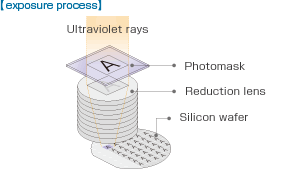
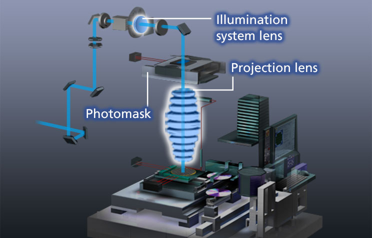
Most modern lithography tools (steppers/scanners) reduce the size of the projected pattern, usually 5× reduction. This does not allow for an increase in the ultimate resolution, but it does make maskmaking a little easier.
Process Bias
When manufacturing semiconductor devices there are a number of things than can shrink or grow your features beyond what the mask defined them to be. For example, if you image a 100 nm line in photoresist and then do an etch on the underlying film, you might undercut the resist and get an 80 nm line when you finish.
Fancy Imaging Tricks
There are a number of "tricks" you can employ in an imaging system to improve resolution beyond what is on the mask. A few names without explaination: dipole apertures, phase shift masks, multiple patterning.
How is it done?
Now, to address your actual question. Masks are made in e-beam or laser direct write systems. A very fine electron beam or laser is used to write patterns into an electron beam or laser sensitive resist and, after developing, is used an an etch mask opening up clear regions in the mask. These systems can write features on the order of 10's of nm but are very slow and expensive. For this reason they are not usually used in production, favoring the faster optical systems.


