3
\$\begingroup\$

I was trying to understand the 2nd answer from this post here, with the circuit of the post shown below. The 2nd answer has equations including open loop gain I wasn't able to understand (1st question).

It has the following equations:

Loop Gain = \$ A_{ol} \frac{R_1}{R_1 + R_F} \frac{1}{s/w_p +1}\$ and \$A_{ol} = \frac{A_{DC}}{(S/W_1+1)(S/W_2+1)}\$

The original post tries to explain why one may want to have a capacitor in parallel with the feedback resistor.

I know that it is to kill the high frequency noise generated from the op-amp.

But if you look at the output of the op amp and see how it would go to the inverting input through the feedback resistor, doesn't the feedback resistor and the parasitic capaitance, Cp, form a low pass filter? (2nd question)

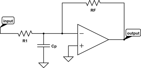
enter image description here

\$\endgroup\$
3
  • \$\begingroup\$ All op-amps have a upper roll-off point due to parasitic capacitance. The parasitic capacitance of Rf is > zero. \$\endgroup\$
    – user105652
    Commented Oct 4, 2018 at 21:53
  • 1
    \$\begingroup\$ To your question: Yes - the feedback function is a lowpass filter.....and that is the problem because it adds additional phase shift to the loop gain and, thus, reduces the stability margin. \$\endgroup\$
    – LvW
    Commented Oct 5, 2018 at 13:45
  • \$\begingroup\$ Continue: What makes a capacitor across RF ? It reduces the loop gain for higher frequencies and can bring the magnitude of the loop gain below unity before the phase reaches the critical value of -180 deg. . \$\endgroup\$
    – LvW
    Commented Oct 5, 2018 at 16:08

2 Answers 2

2
\$\begingroup\$

looking at the original post, the capacitance at the input is due to the large input devices plus wiring and not there by design. This cap adds the pole indicated in the loop gain relation wp. If the amplifier has two additional poles then stability must addressed due to three poles in the loop gain function. A cap in parallel with the feedback resistor adds a zero to the net transfer function and can be positioned to add phase to improve the phase margin.

\$\endgroup\$
0
\$\begingroup\$

You don't want to put the capacitor there between the negative input and ground, because that node is a virtual ground. In a perfect world, that capacitor would have no effect, because the negative input stays at the same level as ground. In reality, there are likely to be stability issues. The capacitor in that schematic represents the parasitic capacitance of the input.

By putting the capacitor in parallel with the feedback resistor, you're not trying to fight the operation of the op amp any more, but reducing its gain at higher frequencies using the feedback path. Even at frequencies where the op amp doesn't respond significantly, it's still a high frequency bypass to a low impedance. This gives greater control overall, including compensating for the parasitic capacitance.

\$\endgroup\$
1
  • \$\begingroup\$ In your answer, it's not apparent what "there" is. Can you clarify? \$\endgroup\$ Commented Oct 5, 2018 at 13:25

Your Answer

By clicking “Post Your Answer”, you agree to our terms of service and acknowledge you have read our privacy policy.

Not the answer you're looking for? Browse other questions tagged or ask your own question.