For example, one pin's name is RA2/AN2/VREF so I wondered what the order is of the functions on this pin. Are they the same or left to right or reverse?
Thank you for your answer.
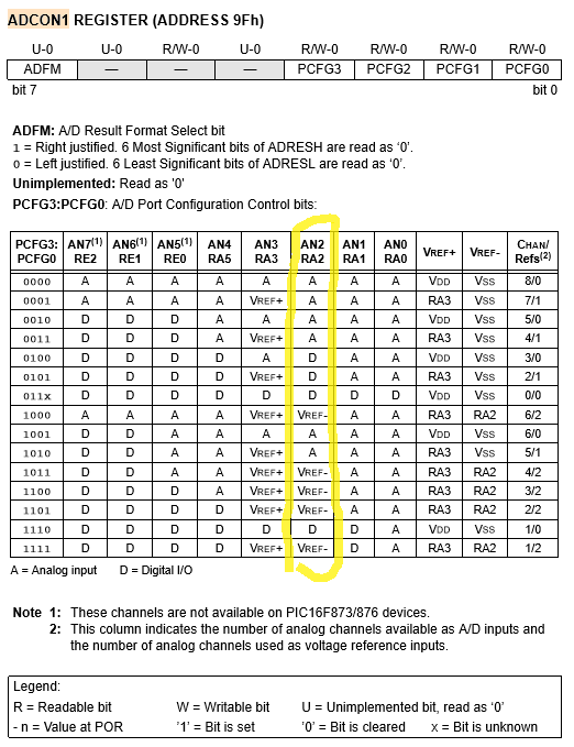
Seems that in general, Microchip I/O ports default to analog input where analog-to-digital converters are available on-chip. This PIC16F877 seems no exception. The configuration of I/O pin function is in 8-bit register ADCON1 (from microchip's pic16f87x data sheet):

Note that upon power-up, register ADCON1 defaults to all 0's, which means that if you do no writing to ADCON1, AN2 is analog input, not digital.
To configure RA2 so that it becomes digital input, you would write to register ADCON1 one of:
where "X" denotes don't care (could be either low or high). If you want RA2 to be digital output, you would also clear a bit in register TRISA.
Awkward? yes...Configuring a limited # of pins for various uses can be confusing, especially so when the methods vary from chip family to chip family. A careful reading of these data sheets is required to see what options are available.
There is no "order of functions" for pins. Pins that are configurable usually have a "default" configuration, and then you can use the control registers to select an alternate function.
So in your example, the pin is named RA2, it probably defaults to GPIO and has alternate functions as analog input 2 or VREF. There is no "order" there, which one it is depends on which configuration you select.
Usually in naming they are given as:
[Name]/[Alternate 1]/[Alternate 2]/.../[Alternate N]
The order that they appear on a symbol is completely up to the person creating that symbol but is usually the same as the data sheet, although some will just put the name (ie RA2) and some may have them in different order. They are the same pin if they have the same name though (you shouldn't have 2 pins with RA2 in them, but you may have 2 pins with AN2).