0
\$\begingroup\$

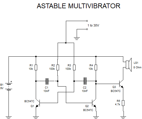
I have trouble understanding the operation of the following circuit:

enter image description here

This is the given description of the schematic:

"This is a voltage controlled multivibrator that is used as an acoustic volt meter. The supply voltage is 9 V and the measure range is also 9 V. At the moment when one of the transistors of the multivibrator starts to conduct, the base voltage of the other transistor drops to -9 V. After this, the 10 nF capacitor is charged by the current through the 100 kΩ resistor to around +0.6 V in approximately 0.65 ms, at which point the circuit switches states."

I am not sure what to 1...30V means here. I don't know what sort of multivibrator circuit this is. As I see it, there are 2 switching capacitors, connected in a feedback network, along with two time delay capacitors. I am not sure how to transistors are biased. Also what happens when the left transistor (Q1) is off? I am also not sure what voltage the collector of Q1 does have and how it affects the capacitors' plates (and thus their voltages).

\$\endgroup\$
3

1 Answer 1

1
\$\begingroup\$

Astable Multivibrator

That circuit is a transistor astable multivibrator.

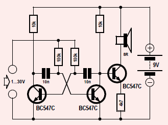
I have redrawn the circuit in order to include some reference letters/numbers on the components.

Start with Q2 just having been switched on with its base at 0.7V and its collector at 0V. Q1’s base will be at -8.3V and will be slowly rising as C2 charges through R3. Simultaneously the collector of Q1 will be rising as C1 charges via R1. The collector of Q1 will reach 9V before its base reaches 0.7V because C1 is charging through a resistance of 10k (R1) whereas C2 is charging through 100k (R3). A little while after the collector of Q1 reaches 9V, its base will reach 0.7V switching Q1 on and forcing its collector to 0V. Voltages across capacitors with a series resistance can’t change instantly and so as the left hand side of C1 drops to 0V, its right hand must also drop by 9V taking the base of Q2 almost instantly down to -8.3V, switching Q2 off and enabling its collector to rise fairly quickly to 9V as C2 charges via R4. A little while later the base of Q2 reaches 0.7V because C1 has been charging via R2. Q2 switches on and its collector drops almost instantly to 0V taking the base of Q1 down to -8.3V. We are back where we started and the above described sequence repeats.

The controlling input voltage is 1 to 30V as shown. The higher this control voltage, the higher the voltage across the 100k resistors and so the higher the charging current through the capacitors as they charge from -8.3V to 0.7V. The higher the charging current, the more quickly the capacitors will charge and therefore the higher the frequency of oscillation. The minimum control voltage is 1V instead of 0V so as to enable the transistors’ bases to rise to 0.7V.

There is a design flaw in that circuit. The bases of the transistors are taken down to -8.3V and the maximum data sheet specified VEB for the BC547 is only -6V! There are a couple of ways around this, lower the supply voltage or add schottky diodes (low forward voltage drop) in series with the transistors’ bases.

\$\endgroup\$

Your Answer

By clicking “Post Your Answer”, you agree to our terms of service and acknowledge you have read our privacy policy.

Not the answer you're looking for? Browse other questions tagged or ask your own question.