0
\$\begingroup\$

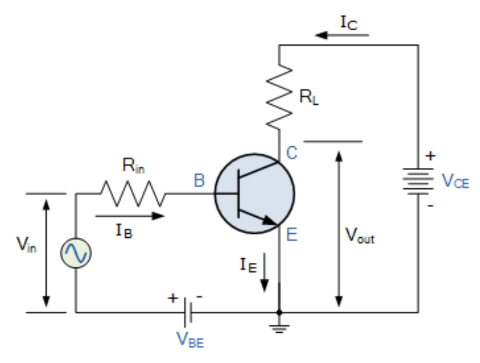
What does the input resistance of a bipolar junction transistor mean? Why is its value equal to the ratio of input voltage to that of base current in the common emitter configuration?

As far as I know, in case of amplifier circuit, a transformer is used to induce signal in tbe circuit. Why is there a resistance which we call input resistance? Is it actually the resistance of the wires?

In my high school curriculum, we are taught about resistance-less wires so I guess the previous question does not make sense then. I could understand that output resistance can refer to a whole different circuit by which the amplified signal can be utilized like for amplifying sound, but why is there an input resistance?

Why is input resistance the ratio of input voltage and base current? If we use Kirchoff's law in the base-emitter loop then shouldn't it be like $$I_B×R_{in}+V_{base-emitter junction voltage}=V_{BE}+V_{in}$$

How is \$R_{in}=V_{in}/I_B\$?

If possible please also let me know why current gain and current amplificatiom factor of a transistor are considered to be constant.

enter image description here

\$\endgroup\$
2
  • \$\begingroup\$ Current gain is not considered to be constant. It varies over 1-2 orders of magnitude depending on how you operate the transistor. \$\endgroup\$
    – tobalt
    Commented Oct 20, 2021 at 11:41
  • \$\begingroup\$ A transformer is not generally used to couple signals in a transistor amplifier. They were used, once, for vacuum tube amplifiers, but transistor-based amplifiers typically use either a capacitor or a direct connection between stages. \$\endgroup\$
    – Hearth
    Commented May 29, 2022 at 18:17

6 Answers 6

1
\$\begingroup\$

Why input resistance is the ratio of input voltage and base current?

Because that is how it is defined and the small signal (incremental) input resistance at the working voltage is the ratio of a small change in input voltage about the working voltage divided by the corresponding change in base current. It is the combined effect of \$R_{\rm IN}\$ and the base-emmiter junction.

\$\endgroup\$
2
  • \$\begingroup\$ Is this resistance something imaginary? \$\endgroup\$
    – MSKB
    Commented Oct 20, 2021 at 13:14
  • \$\begingroup\$ @MSKB Some people might tell you that there is no such thing as a dynamic emitter resistance and that the quantity dVbe/dIbe = 25mV/Ie should always be referred to as 1/gm which is the inverse of the transconductance! \$\endgroup\$
    – user173271
    Commented Sep 27, 2022 at 11:38
1
\$\begingroup\$

Bipolar junction transistors have no input resistance.

An input resistance can be defined for ports of n-port networks, such as the common-emitter configuration you've shown, with the two terminals connected to \$V_{in}\$ being one such port. If you connect an ideal voltage source \$V_{in}\$ to such a port, resulting in a current flow \$I_{in}\$, the input resistance is defined to be

$$ R_{in} := \frac{V_{in}}{I_{in}}.$$

Applied to your common-emitter circuit, we get \$ R_{in} = V_{in} / I_B \$.

For DC inputs, \$R_{in}\$ varies strongly with \$V_{in}\$ (in this case) - the input resistance will be large for voltages below the BE-diode's forward voltage and very low for voltages above the forward voltage. You call this the large signal input resistance.

When used as an amplifier, one would bias the BJT suitably with a DC voltage to put it into the linear region and superimpose a small AC signal to be amplified. In this case, the small signal input resistance \$r_{in}\$ is of interest. You can calculate \$r_{in}\$ from a small-signal model of a BJT and the various transistor parameters that can depend on the biasing conditions. Any textbook on BJTs or amplifier circuits should cover that.

As for your circuit diagram: I think it is misleading. \$R_{in}\$ should probably not be in there. It is voltage-dependent and thus not an actual resistor, and if you considered it a voltage-dependent resistor, it would also incorporate the BE diode.

Regarding the (common-emitter) current gain \$\beta\$: it is roughly constant only in the linear region of the BJT. (If it were not, there would be no linear region, so this is just a tautology.)

\$\endgroup\$
2
  • \$\begingroup\$ I thought $R_{in}$ to be a resistor. Is R_{in} a hypothetical concept which does not exist but we consider that it does? \$\endgroup\$
    – MSKB
    Commented Oct 20, 2021 at 13:18
  • \$\begingroup\$ In the case of your schematic, it is hard to tell without context. Maybe they are disregarding the BE junction and placing an actual resistor \$R_{in}\$ in there, which would then be the input resistance of the circuit. This would be valid for large input voltages. Or maybe it is really supposed to be the small-signal input impedance. In any case, for the general common-emitter circuit (as can be seen here), the large-signal \$R_{in}\$ is definitely not constant. \$\endgroup\$ Commented Oct 21, 2021 at 12:12
1
\$\begingroup\$

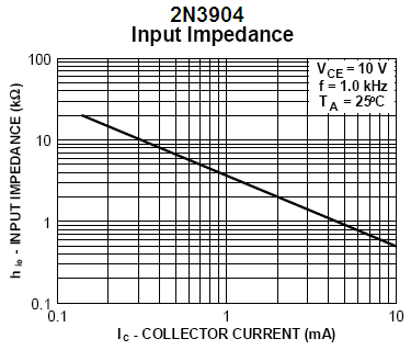
The datasheet of a 2N3904 transistor has a graph of its typical input impedance vs collector current: 2N3904

\$\endgroup\$
1
  • 1
    \$\begingroup\$ Hi, Please add a link to the specific document where that image came from. Thanks. \$\endgroup\$
    – SamGibson
    Commented Sep 27, 2022 at 15:09
0
\$\begingroup\$

There is a confusion regarding the term Rin.

When the fixed resistor Rin as shown in the circuit is part of the question, the ratio Vin/In is NOT identical to this resistor Rin.

1.) The total DC input resistance of the circuit is the sum of Rin plus the DC ratio Vbe/Ib. Only the last part of the sum is the DC input resistance "of the transistor".

Comment: When we speak about the input resistance of a transistor (or a complete circuit) in most cases, we mean the ac input resistance rin.

2.) The ac input resistance of the shown circuit is rin=(Rin + hie) .

The term hie is the ac input resistance at the base node. This resistance is identical to the slope of the input charcteristic Ib=f(Vbe).

This slope is found to be hie=Vt/Ib.

It also can be calculated by the ratio (current gain)/(transconductance): hie=hfe/gm.

\$\endgroup\$
2
  • \$\begingroup\$ Is rin the dynamic resistance of base-emitter junction? My textbook indirectly suggests that, so need to be sure. \$\endgroup\$
    – MSKB
    Commented Oct 20, 2021 at 14:15
  • \$\begingroup\$ No - not necessarily. The resistance rin is the dynamic input resistance of a circuit or an active device. It is always necessary to DEFINE the node where rin is referenced to. Sometimes it is the input resistance at the base - and some times (as in your example) at the input node of a circuit: As I have written: rin=(Rin + hie). Here, the term hie is the dynamic resistance between base and emitter. It really depends on the specific application - and must be defined !! \$\endgroup\$
    – LvW
    Commented Oct 20, 2021 at 15:27
0
\$\begingroup\$

AC input resistance of the transistor = dVbe/dIb = re(1 + beta) where re = dVbe/dIe = 25mV/Ie (at 25 degreesC).

re is the intrinsic emitter resistance otherwise known as the dynamic emitter resistance.

AC input resistance of complete circuit = Rin + re(1 + beta).

Beta = hFE which is the transistor's current gain = Ic/Ib

\$\endgroup\$
0
\$\begingroup\$

Here is part of Fairchild's 2N3904 datasheet:

2N3904 datasheet

\$\endgroup\$
1
  • \$\begingroup\$ You should add this information editing your other answer, not posting a non-answer like this. \$\endgroup\$ Commented Oct 6, 2022 at 15:49

Your Answer

By clicking “Post Your Answer”, you agree to our terms of service and acknowledge you have read our privacy policy.

Not the answer you're looking for? Browse other questions tagged or ask your own question.