2
\$\begingroup\$

I need to check the resistance of a test point (TP) through a 4 wire system. I know and understand the theory behind it, but how do I put it into an Altium schematic? I have the voltage measurement channel available but the sense connection is little bit confusing.

Is there a screenshot of an example schematic, preferably in Altium?

P.S I am designing an adapter which has a tester PCB to test one product (DUT).

\$\endgroup\$

2 Answers 2

2
\$\begingroup\$

Typically you would use a net tie to use separate traces for the main and sense connections, and then tie them together at the measurement point (in this case, your test point). Altium's documentation explains net ties in further here.

The linked documentation shows a case of connecting two different ground nets together at a specific point:
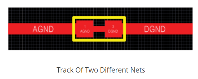
Altium net tie PCB

These AGND and DGND nets would be analogous to your main and sense connections.

In the schematic the net tie looks like this (also from the linked documentation):
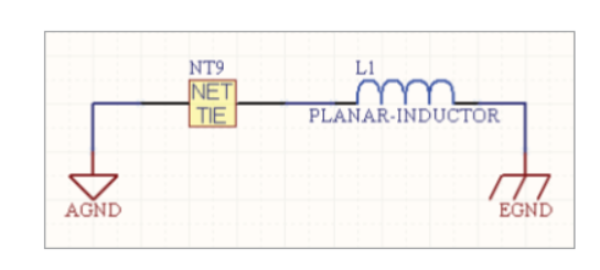
Altium net tie schematic

The net tie can be designed to have a footprint on the top or bottom of the board (like an 0805 size) so that you can potentially cut the trace between the two nets and insert a component (like a resistor), or it can be a logical connection only (you can even make the connection on an inner layer, if desirable).

Here is an example of an inner layer net tie (no footprint, no BOM component, and implemented just like a normal trace):
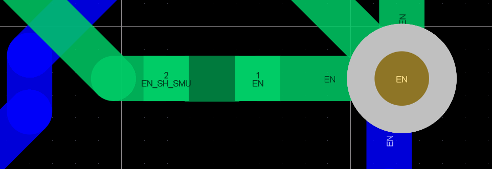
enter image description here

In this case I'm using a Kelvin connection for applying a voltage to an enable pin (EN). The EN net is the force connection, and the EN_SH_SMU is the sense connection. The DUT is not shown but it's just to the right of the EN via.

You would need two net ties, one to tie your high side main/sense connections together, and one to tie your low side main/sense connections together.

\$\endgroup\$
3
  • \$\begingroup\$ Thanks for the answer. Is it possible that you can show how to do it? \$\endgroup\$
    – Theta
    Commented Nov 4, 2021 at 15:14
  • \$\begingroup\$ @Hassan Altium's documentation is far more extensive than I could give, and Altium will have the documentation for whatever version you are using (the version shouldn't matter much, but the process could change from version to version). \$\endgroup\$
    – Null
    Commented Nov 4, 2021 at 15:18
  • \$\begingroup\$ I am not able to put this into schematics part, in pcb editor, I can manage. I have seen how to use the net ties and their functionality is clear. \$\endgroup\$
    – Theta
    Commented Nov 4, 2021 at 15:30
0
\$\begingroup\$

enter image description here

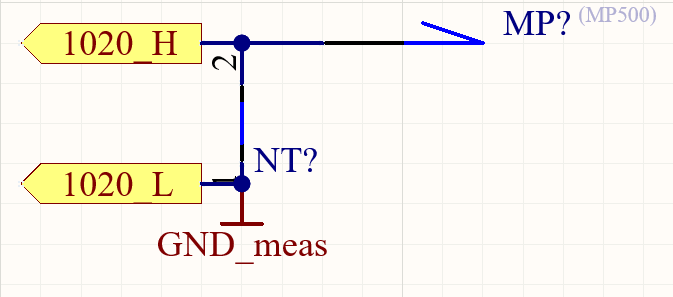
1020_H and 1020_L are going to the measurement channels. Net tie is used to connect them. This solution could work.

\$\endgroup\$

Your Answer

By clicking “Post Your Answer”, you agree to our terms of service and acknowledge you have read our privacy policy.

Not the answer you're looking for? Browse other questions tagged or ask your own question.