2
\$\begingroup\$

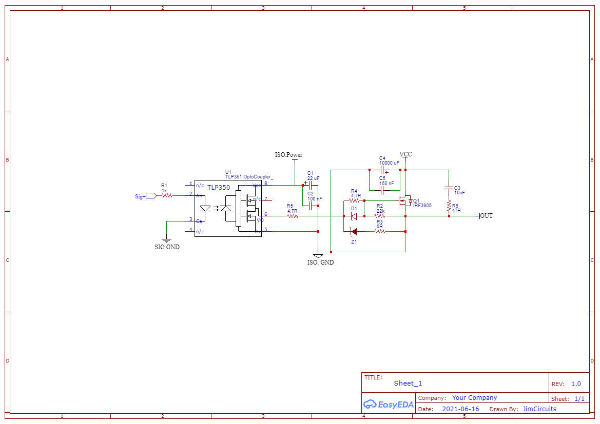
Quarter BridgeI am in the process of building a low frequency (that is, transformer based) pure sine wave power inverter; 24 VDC to 120/240 60 Hz AC. The schematic I've attached is for one quarter of the entire bridge; all the other quadrants are identical. Progress so far has been to implement SPWM from an Arduino Nano, driving a pair of IRF21844 half bridge MOSFET drivers. Those drivers subsequently drive TLP351 opto gate drivers. There is independent 12 V isolated power supplies to each high side quadrant and the two low side quadrants share a power supply.

The TLP351 output passes through a 4.7 ohm gate resistor that is in parallel with a reverse biased Schottky diode. Each FET has a 22 kohm gate-source resistor. The FETs themselves are IRF3905 with two per quadrant. All of this works pretty good to drive resistive loads or even brushed AC motors, but even small induction motors blow the FETs. I've managed to alleviate this somewhat by putting 15 V zener diodes from source-to-gate, but even then, if I rapidly switch the motor, I'll occasionally blow some FETs.

I've got the parts on hand to make some RC snubbers between the drain-source of each FET, but haven't done that yet. I was relying/hoping the FET body diode would suffice, but I don't think it is.

My question is, assume parts count wasn't an issue, how would you make the ultimate bulletproof H-bridge. Keeping the driving components the same, what would you add to the H-bridge to make it the best possible bridge?

Edit to describe logic drive:

I've added a schematic to the OP. I'll try to address your points, @bobflux. The 24 V is from four 215 AH 6 V lead acid deep cycle batteries charged by a 435 watt solar panel. So no automotive shenanigans. I am using isolated drivers because I want the FET board as electrically isolated from the driver board as possible. The driver design is pretty much a done deal. There is a bootstrap diode and cap available and originally that is how I started. But I found out pretty quickly that one small misstep with a scope or meter probe, or even just regular testing that blows a FET will also kill the IRF21844s and maybe even the Arduino Nano. So I now use isolated gate drive supplies and TLP351 opto drivers. The IRF21844s still handle the dead time and they have a shutdown pin that will eventually be used with a CT and hardware amplifier for rapid shutdown. I haven't put any of that to use YET because I am still working the bridge bugs out.

\$\endgroup\$
4
  • 5
    \$\begingroup\$ Welcome! Please post a schematic. \$\endgroup\$
    – winny
    Commented May 11, 2022 at 18:02
  • \$\begingroup\$ Measure the gate with a scope to make sure that there isn't any ringing going on, and that the 4.7Ω isn't too large, causing slow turn on. \$\endgroup\$
    – Aaron
    Commented May 11, 2022 at 18:47
  • \$\begingroup\$ Do you really want a pure sine wave without any PWM switching? A pure analog solution with a lot of heat loss in the H bridge and a pour efficiency? \$\endgroup\$
    – Uwe
    Commented May 11, 2022 at 19:02
  • \$\begingroup\$ I'm not sure what you mean. The answer is no, obviously. The switching is PWM, sinusoidal PWM at 24 kHz. A choke on the transformer primary and filter capacitor on the secondary filter the PWM and the resultant sine wave is quite clean... Until I blow it up. \$\endgroup\$ Commented May 11, 2022 at 19:11

3 Answers 3

2
\$\begingroup\$

I've been thinking about a couple of approaches to doing this.

The cognoscenti seem to go with stepping up the DC to a high voltage (165V for 120V/60Hz, or 330V for 230V), then using a high-voltage direct PWM to make the output without a transformer. And indeed you can find lots of literature and examples of that kind of topology; it's also what's used for motor drives too and some Class D amplifiers. The advantage is that the step-up can use a high frequency and thus lower inductance, saving cost, weight and size. The whole point of using newer devices like GaN and SiC IGBTs is to be able to deal with these high voltages directly. Your design could leverage the work in this area.

The second approach, which is kind of what you're doing, is to treat the AC signal as if it were a bridged Class D amplifier feeding a transformer. I think it's laudable that you're doing this, as it can enhance the safety of your inverter by allowing the secondary to float. The downside is that the final transformer needs to support very large primary currents, yet have large enough inductance to work at the low frequency required. This will make the converter more bulky overall: the primary windings need to be big to handle the current, as does the core for the needed inductance.

I think a middle path might be better. I like the idea of having isolation, but how to make the transformer more... reasonable? Here's the idea: step your 24VDC up to 84VDC (3.5x) using a flyback or other suitable topology. Then run a bridged Class D from that DC rail to make a ~168V differential swing. Then feed that to a 1:1 transformer to get the isolation. By dividing up the work, both the step-up and isolation transformer primary currents and voltages are a bit more manageable.

\$\endgroup\$
1
  • 1
    \$\begingroup\$ Yes, the "high frequency" vs "low frequency" topology. The first inverter I built was of this type. It works very well. The drawback is that the small high frequency transformers used in those kinds of inverters just don't have the "inertia" to start inductive loads. A store bought reputable high frequency sine wave inverter can be easily killed by a relatively small induction motor. High frequency inverters have about a 2x surge rating vs. a low frequency transformer based inverter that can surge 4x or 6x. Granted, I never tried the hybrid topology you suggest. \$\endgroup\$ Commented May 11, 2022 at 22:46
1
\$\begingroup\$

You need to ensure you have non-overlap on the HS and LS FETs in the H-Bridge.

With an inductive load, you also need to ensure you have sufficient V rating for your FETs, and also that the VCC and GND are well decoupled -- many MLCC (ceramic) capacitors placed v. close to the FETs, slightly larger caps next to those etc. The values needed will depend on the V and I you are using.

\$\endgroup\$
2
  • \$\begingroup\$ I will post a schematic when I get home. I didn't mention it, but there are four 10000 uF capacitors basically on top of the FETs each with a 0.15 uF tantalum cap in parallel. Should I have used ceramic? Also, there is about 300 ns of dead time between upper and lower FETs, I haven't observed any shoot through, but I only have a secondhand 20 MHz USB oscilloscope, so I may be missing something. \$\endgroup\$ Commented May 11, 2022 at 18:37
  • 1
    \$\begingroup\$ @NickLacarno ceramic are much better for this than tantalum. The ESR is much much lower, and they don't catch fire like tantalums do. \$\endgroup\$
    – Aaron
    Commented May 11, 2022 at 18:46
0
\$\begingroup\$

If the 24V is really 24V, and not automotive 24V than can get a lot higher, I'd use a pair of cheap half-bridge MOSFET drivers with integrated adaptive dead time like NCP5901, ADP3120, ADP3110, etc. If the "24V" can get a bit higher, then something higher voltage like DGD05473. IRF21844 is also a good choice, a bit high voltage, but that's not really a problem.

Then a bunch of MOSFETs of proper RdsON for the desired current. Since PWM frequency will be pretty low, no need to switch in 10ns, so adequate gate resistors should be chosen. Not too high to minimize switching losses, but not too low either to avoid unnecessary EMI or MOSFET oscillations. Probably something like 33-51R.

I don't understand why you're using isolated gate drivers since the MOSFETs sit on the same power supply as the driver. You're using PWM, so a bootstrap driver should work just fine.

Then perhaps a small LC filter, maybe doubling as a common mode filter, to remove the worst of the HF before it hits the transformer, so it doesn't radiate.

A very low value shunt resistor (or just a PCB track) in the ground connection, with a fast comparator to implement a current limit. This should abort the current PWM cycle if exceeded, but not latch. This is to allow a sort of inrush current limiting for difficult loads like induction motors, which draw a huge current at start-up. It's best to do it in hardware, not software, because hardware protections are still active when the code is frozen in a debugger breakpoint. The triggering current should be below the transformer saturation current, because if the transformer saturates, the MOSFETs will have a bad day.

Then, perhaps, a way for the microcontroller to know it triggered, so it can decide to give up and stop if the overcurrent protection triggers for longer than would seem reasonable, which would indicate a short on the output instead of motor inrush current.

Basically, this hardware protection deals with very quick stuff that can eject the MOSFETs from the board, but you also need to protect them against overheating and cooking. So, a temperature sensor, and something that measures average current, with software monitoring it.

Now if your MOSFETs blow up, it could be because of excessive inrush current in your induction motor (hence the protections above) or because of voltage spikes. The only cure for those is low inductance layout and ceramic caps, to make sure your power rail has very low inductance to ground, so the sharp current variations from MOSFET switching do not create unwanted spikes. e=L di/dt, so if di/dt is high, you must have low L. Large electrolytics have high inductance (>10nH) so you need SMD ceramics, in the µF range, which also have very low ESR. Note the inductance of the MOSFET leads also counts, so SMD or short leads and short traces are better.

\$\endgroup\$
1
  • \$\begingroup\$ Edited my OP to address your questions. \$\endgroup\$ Commented May 12, 2022 at 1:11

Your Answer

By clicking “Post Your Answer”, you agree to our terms of service and acknowledge you have read our privacy policy.

Not the answer you're looking for? Browse other questions tagged or ask your own question.