0
\$\begingroup\$

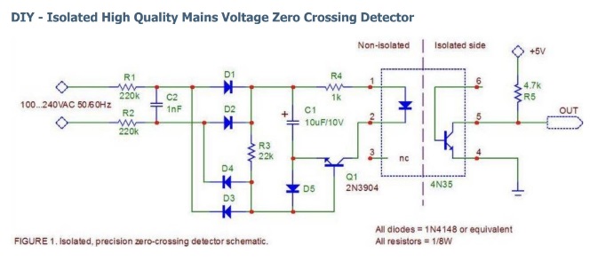
I was reviewing some zero crossing detector circuits and found on this page the following circuit:

enter image description here

I have knowledge of the operation of the devices individually, but I can't understand their mathematical description well, and I have seen that in another forum on this page they explain the operation of this circuit, but I don't want to know just how it works, I want to know how it can describe its behavior mathematically, could someone help me analyze the circuit and find a mathematical model? I don't mean to use differential equations or things like that, just apply node laws or Kirchhoff's laws and thus be able to calculate the values ​​of the electrical components . I hope you can help me, thank you.

\$\endgroup\$
4
  • \$\begingroup\$ Actually I don't see how this would work very well at all, and I suggest that you draw the circuit in a simulator and see what it does. The rectifiers will charge the capacitor to about 10V with 220 VAC input (so it should be rated at least 16V). The optoisolator would turn on when the transistor is biased ON, but I don't see where that would happen. Can you post the link to the source and explanation? \$\endgroup\$
    – PStechPaul
    Commented Dec 2, 2022 at 0:46
  • 2
    \$\begingroup\$ Please look at this question that I answered: electronics.stackexchange.com/questions/468317/… \$\endgroup\$ Commented Dec 2, 2022 at 1:33
  • \$\begingroup\$ @Kevin White - I found the circuit in the question you solved, your answer seemed the best of all, but how could I get some equations to know (at least theoretically) the expected voltage values ​​or the charge and discharge times of the capacitor \$\endgroup\$
    – WalterPH
    Commented Dec 2, 2022 at 4:21
  • \$\begingroup\$ @KevinWhite - you mentioned that the pulse time is approximately 1ms but... how did you calculate that value? How could I calculate the current that flows through the collector of the transistor? If I wanted to use another optocoupler than the 4N35, how does it affect the rise time or CTR? Could you tell me how to proceed to find the most relevant equations of the circuit and thus obtain theoretical approximations of the ideal values ​​in case I want to change any component or something like that? I would really like to be able to calculate some things in this circuit \$\endgroup\$
    – WalterPH
    Commented Dec 2, 2022 at 4:23

1 Answer 1

0
\$\begingroup\$

I don't mean to use differential equations or things like that, just apply node laws or Kirchhoff's laws and thus be able to calculate the values ​​of the electrical components

The first step in analyzing this circuit is to simplify. R1 and R2 can be combined into a single resistor. C2 is small enough that at 50~60 Hz it will have negligible effect. D1..D4 can be replaced with a rectified sine wave and single blocking diode. We will assume that D5 and Q1 B-E junction have a voltage drop of ~0.7 V, and that the optocoupler LED has a voltage drop of 1.1 V. The simplified circuit then looks like this:-
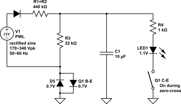
schematic

simulate this circuit – Schematic created using CircuitLab

Now it is easier to see what role each component plays and what effect its value has on the zero-cross detection timing.

R1+R2 and R3 form a voltage divider that reduces the rectified mains voltage, and R1+R2 in parallel with R3 is the effective series resistance that determines how fast C1 charges (use Thévenin's theorem to derive the equivalent voltage and resistance).

When the mains voltage is close to zero the rectified input voltage drops below the voltage on C2, causing Q1 to turn on and switch R4 and LED1 across the capacitor which discharges it faster, until the input voltage rises at the end of zero crossing and turns Q1 off.

If Q1 never turned on the voltage on C1 would center around the average voltage of the rectified input waveform (2Vpk/π), less 1 diode voltage drop through D5/Q1. However with Q1 turning on during zero crossing the average capacitor voltage drops due to faster discharge through R4 and LED1. Capacitor voltage is needed to determine the value of R4 required for the desired LED current, but the calculation is complicated by interaction with the pulse ratio (and you wanted to avoid differential equations).

While you could develop a formula that includes all the required parameters, it will probably be a lot easier and less error-prone to simulate it using a program such as LTspice.

\$\endgroup\$
7
  • \$\begingroup\$ Your answer really helped me understand a bit more, actually I would think diode D5 would be in series with capacitor C1 but I'm not really sure, could you tell me why diode D5 is not in series with capacitor C1 in your simplified model ? If you can't, I'm still very grateful for taking the time to help me with your answer. \$\endgroup\$
    – WalterPH
    Commented Dec 2, 2022 at 22:48
  • \$\begingroup\$ It is. Follow the current path from V1+ through R1+R2, C1, D5 and back to V1-. Don't be fooled by the 'ground' - it's just an arbitrary reference point chosen to make the circuit look more conventional. \$\endgroup\$ Commented Dec 2, 2022 at 23:16
  • \$\begingroup\$ Remember too that while this current flows the voltage at D5 cathode is negative relative to 'ground', turning Q1 off. Only when V1 falls below the voltage on C1 does the current reverse, causing positive voltage at D5 cathode. Q1 is turned on from C1 via current going through R3 (V1 being effectively disconnected at this point because the blocking diode is reverse biased). \$\endgroup\$ Commented Dec 2, 2022 at 23:17
  • \$\begingroup\$ Which reminds me that the value of R3 should be chosen to provide a suitable amount of Base current. Yet another variable! \$\endgroup\$ Commented Dec 2, 2022 at 23:20
  • \$\begingroup\$ @WalterPH You said (as Bruce points out) that you don't want to involve differential equations. Yet it actually is the fact that a capacitor's current peaks when the slope of the voltage changes across it are at a maximum. And this peak occurs once every half-cycle of the AC input. The fact that the two diodes (one actual and one from the BJT) "clamp" one end of the capacitor while the other end is exposed to the rectified AC is what yields this peak right at the zero-crossing. It is exactly this differential understanding which explains why it works right at the AC zero-crossing. \$\endgroup\$
    – jonk
    Commented Dec 3, 2022 at 20:23

Your Answer

By clicking “Post Your Answer”, you agree to our terms of service and acknowledge you have read our privacy policy.

Not the answer you're looking for? Browse other questions tagged or ask your own question.