5
\$\begingroup\$

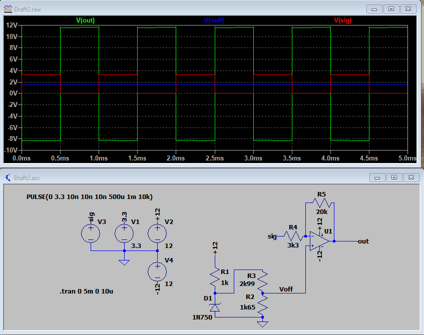
I'm trying to make a neat and obvious circuit for amplifying a 0-3.3V PWM signal to -10/+10V. I'm able to adjust the gain and feed the signal on the inverting end. I also want to add a 1.65V (3.3V/2) offset to the non-inverting pin so I can pull the signal to -1.65/+1.65 V range before applying gain, but the op-amp seems to just not add the exact offset voltage I'm creating with the Zener-potentiometer reference voltage circuit on the bottom middle of the schematic. There is some extra unwanted offset in the output.

I'm not well knowledgeable in analog electronics so there might be something very essentital I'm missing. I'm just trying to keep everything obvious in the circuit so I can understand what's going wrong in the circuit, but it seems like the op-amps just don't work the way I think they do. I used to think they add the voltage in the non-inverting input. I've checked a few schematics for offset adjustable op-amp circuits but wasn't able to comprehend. Can someone tell me why my logic in this circuit is wrong and what would be the modifications to make this work?

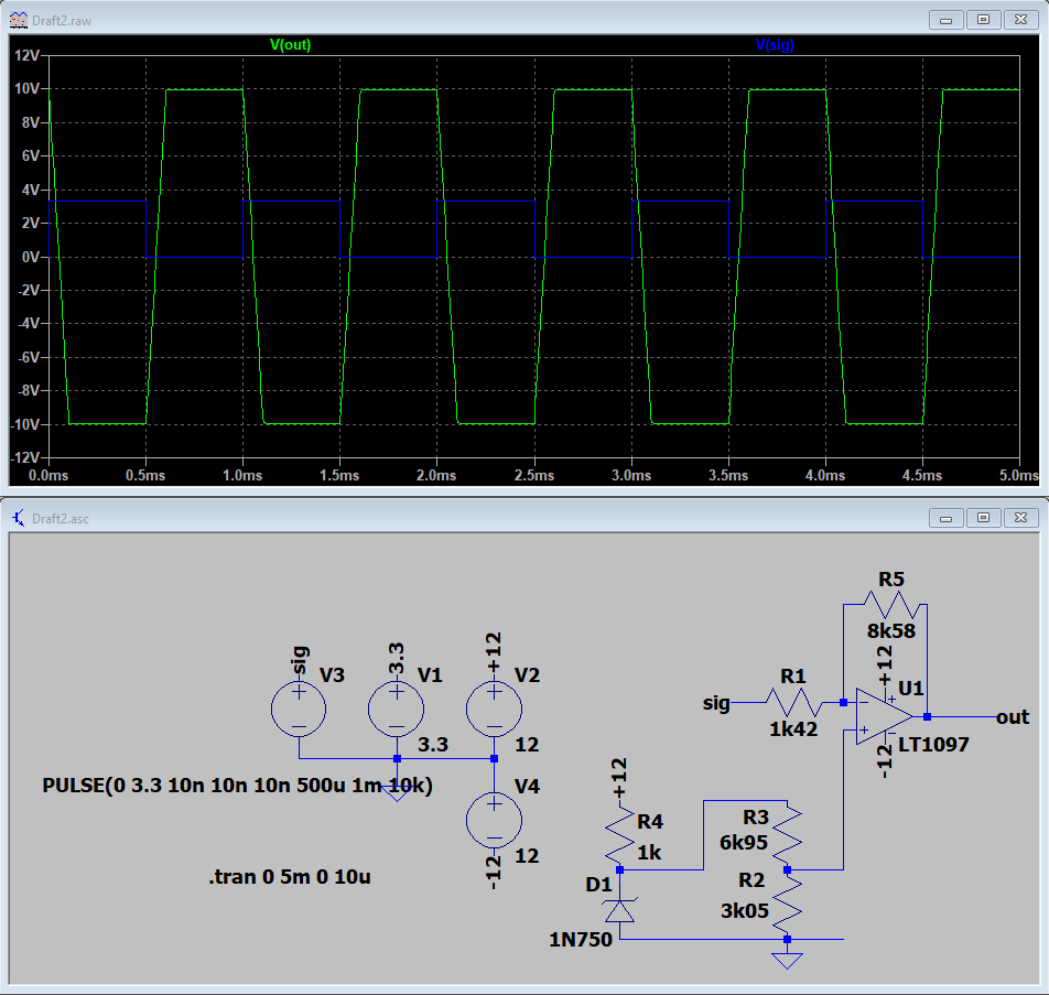
Below is the circuit I've designed, the input signal, offset voltage and the output voltage.

Note: The "3.3" node is a stray node used for a previous design.

LTspice screenshot

\$\endgroup\$
4
  • \$\begingroup\$ What's the voltage on the 1N750 reference, and on the opamp non-inverting pin? If the latter is 1.65 V, then you have a nice 3.3 V input swing centred around 1.65 V, becoming a nice 20 V swing, also centred around 1.65 V. \$\endgroup\$
    – Neil_UK
    Commented Jun 10, 2023 at 15:56
  • \$\begingroup\$ Do you intend to invert the output or should it be in phase with the input? \$\endgroup\$ Commented Jun 10, 2023 at 16:03
  • \$\begingroup\$ @Neil_UK , 1N750 zener is rated at 4.7V reverse breakdown and the non-inverting pin voltage is at 1.65V, as presented by the blue V(voff) in the graph. So, hmm, should I just simply connect the non-inverting pin to ground? Then the output should have a 20V swing around 0 volts from what I inderstand from your suggestion. \$\endgroup\$ Commented Jun 10, 2023 at 20:50
  • \$\begingroup\$ @EdinFifić , I have the option to invert the signal back at the receiver(servo drive), and also as I always heard to always use the inverting pin of an op-amp for the signal(don't know why but they say the performance is better), I used the inverting pin for the signal. \$\endgroup\$ Commented Jun 10, 2023 at 20:52

4 Answers 4

7
\$\begingroup\$

I've written up three approaches to achieve want you want. The first answers your questions, the second shows you a simpler alternative, and the third is a non-inverting solution.


1. What causes the the unwanted offset

It helps to examine behaviour from a purely algebraic perspective:
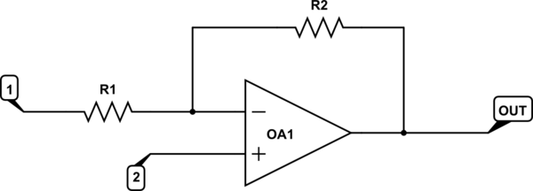
schematic

simulate this circuit – Schematic created using CircuitLab

This arrangement has the following relationship between inputs \$V_1\$ and \$V_2\$, and output \$V_{OUT}\$:

$$ V_{OUT} = V_2\left(1 + \frac{R_2}{R_1}\right) - V_1\frac{R_2}{R_1} $$

The gain \$G\$ you require as you vary \$V_1\$ will need to be:

$$ G = \frac{(+10V)-(-10V)}{(+3.3V)-(0V)} = 6.06 $$

This must correspond to the coefficient of \$V_1\$, which is \$-\frac{R_2}{R_1}\$, and which in your case is \$-\frac{20k\Omega}{3.3k\Omega} = -6.06\$. That's the right magnitude, at least, but the change of sign indicates that "0V to +3.3V" input will correspond to "+10V to -10V" respectively, an inverting behaviour.

Your values of R5 and R4 are fine.

Whatever fixed potential \$V_2\$ you apply at node 2 is multiplied by coefficient \$1 + \frac{R_2}{R_1}\$. Clearly, setting \$V_2=+1.65V\$ will not produce the offset you expected. The assumption that +1.65V will do, is your source of grief.

To find an appropriate value for \$V_2\$, you must solve the equation above for some set of known conditions that you are aiming for. For example, when \$V_1=+1.65V\$, then we require \$V_{OUT}=0V\$. Plugging those values into the above equation:

$$ \begin{aligned} V_{OUT} &= V_2\left(1 + \frac{R_2}{R_1}\right) - V_1\frac{R_2}{R_1} \\ \\ 0 &= V_2\left(1 + \frac{20k}{3.3k}\right) - 1.65\frac{20k}{3.3k} \\ \\ 0 &= 7.06V_2 - 10 \\ \\ V_2 &= 1.42 \end{aligned} $$

Knowing the required potential at the non-inverting input, choose R3 and R2 such that you derive +1.42V from your +4.7V zener reference:

$$ 4.7 \times \frac{R_2}{R_2+R_3} = 1.42 $$

You might end up with this:
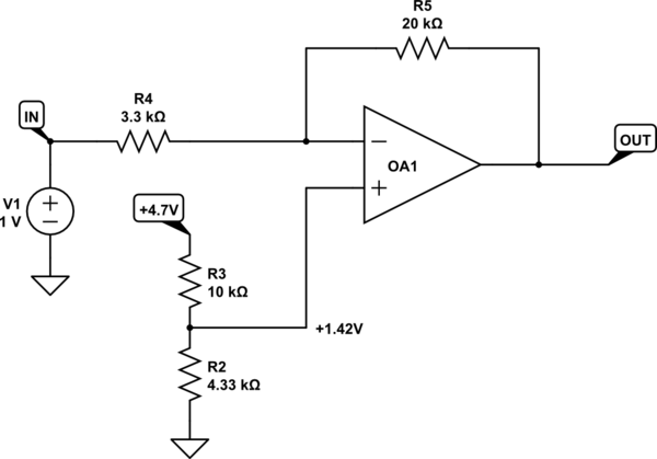
schematic

simulate this circuit

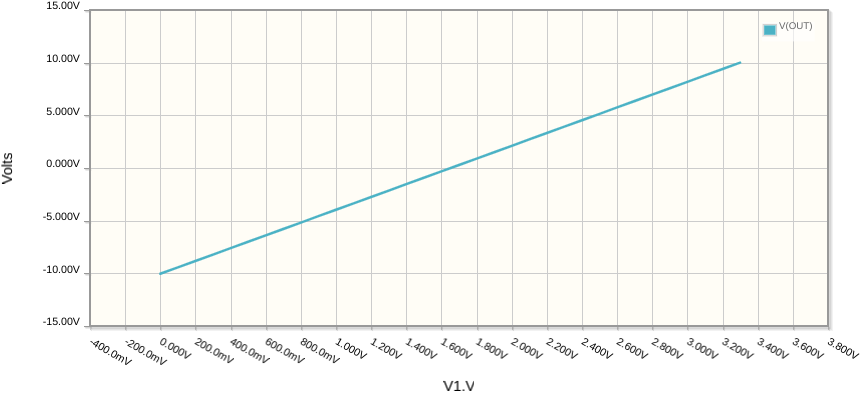
This is the relationship between \$V_{IN}\$ and \$V_{OUT}\$:
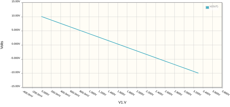
enter image description here


2. Use a summing amplifier

Since you mentioned that being "obvious" is one of the design criteria, there is a another way, that doesn't require such an obscure and strange figure of 1.42V.

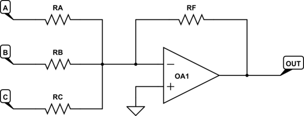
Employ an inverting summing amplifier:
schematic

simulate this circuit

It's called a summing amplifier because of its input/output relationship:

$$ V_{OUT} = -R_F\left(V_A\frac{1}{R_A} + V_B\frac{1}{R_B} + V_C\frac{1}{R_C}\right) $$

or

$$ V_{OUT} = -\left(V_A\frac{R_F}{R_A} + V_B\frac{R_F}{R_B} + V_C\frac{R_F}{R_C}\right) $$

There can be as many input branches as you want, but your application only requires two, a source signal (0V to +3.3V), which I will call \$V_A\$ and some offset which I will call \$V_B\$. Our equation looks like this:

$$ V_{OUT} = -\left(V_A\frac{R_F}{R_A} + V_B\frac{R_F}{R_B}\right) $$

The coefficient multiplying \$V_A\$ is 6.06, as we established before, and this can be achieved using the same resistances 3.3kΩ and 20kΩ we used before. That gives us:

$$ V_{OUT} = -\left(V_A\frac{20k}{3.3k} + V_B\frac{20k}{R_B}\right) $$

As before, we need to find values for \$R_B\$ and \$V_B\$ that satisfy a known set of conditions. Again I'll use conditions \$V_A=+1.65V\$ and \$V_{OUT}=0V\$, since that zero will simplify the arithmetic:

$$ \begin{aligned} 0 &= -\left(1.65 \times 6.06 + V_B\frac{20k}{R_B}\right) \\ \\ \frac{V_B}{R_B} &= -\frac{10}{20k} \\ \\ \end{aligned} $$

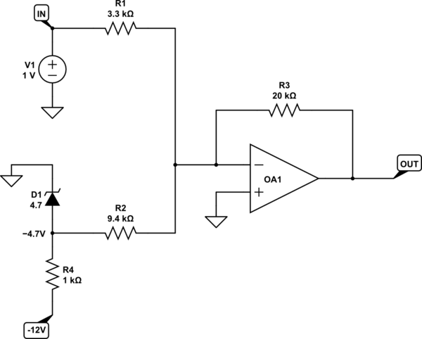
Since \$R_B\$ is necessarily positive, this implies that we need \$V_B\$ to be negative. You have a zener diode, and a −12V supply, and that will allow us to produce \$V_B=-4.7\$ very easily. So now we can find a corresponding \$R_B\$:

$$ \begin{aligned} \frac{V_B}{R_B} &= -\frac{10}{20k} \\ \\ R_B &= -\frac{-4.7 \times 20k}{10} \\ \\ &= 9.4k\Omega \end{aligned} $$

The resulting circuit is this next one, having the exact same response to \$V_{IN}\$ as the previous circuit:
schematic

simulate this circuit

Its behaviour is easier to understand, because anyone familiar with summing amplifiers will take one look at this circuit and immediately see the relationship:

$$ \begin{aligned} V_{OUT} &= -\left(V_{IN}\frac{20k}{3.3k} + (-4.7V)\frac{20k}{9.4k}\right) \\ \\ &= -\left(6.06V_{IN} - 10V\right) \\ \\ \end{aligned} $$

I took you through a somewhat complex algebraic approach, because I couldn't think of a better way to conclude that your offset reference of 4.7V needs to be negative. However, looking at the summing formula, I'm pretty sure you can see that the ratios \$\frac{R_F}{R_A}\$, \$\frac{R_F}{R_B}\$ etc are really just "weights" applied to each input potential, which makes deriving the required resistances in practice much more trivial than I've shown here.


3. A non-inverting alternative

You could stop there, question answered. But what if you wanted a non-inverting version? Let's consider this input to output relationship:

$$ V_{OUT} = 6.06 V_{IN} - 10 $$

That's the same expression multiplied by −1, so you could just add another inverting stage:
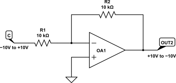
schematic

simulate this circuit

That will work, but it requires another op-amp and two more resistors. The same relationship can be achieved with a single op-amp, but it requires an understanding of Thevenin Equivalence, and some more involved algebra. As usual, let's start with a boiler-plate design, and a formula that relates input to output:
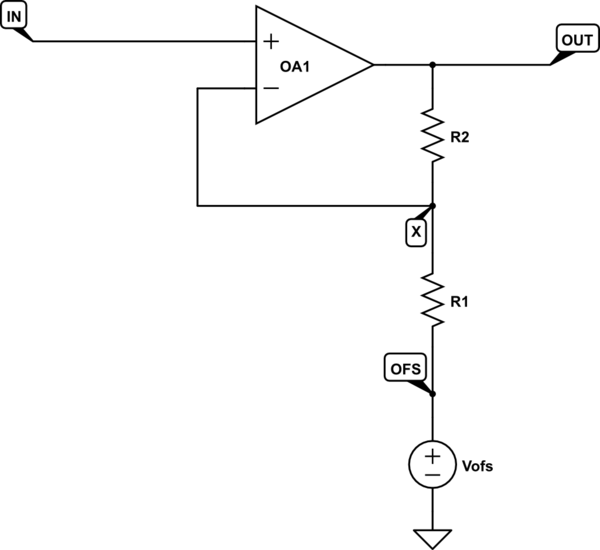
schematic

simulate this circuit

$$ V_{OUT} = V_{IN}\left(1+\frac{R_2}{R_1}\right) - V_{OFS}\frac{R_2}{R_1} $$

If that looks familiar, it's because it's the same as the very first formula at the top of this answer. We're just swapping the points where we apply our signal and our DC offset.

First step is to figure out resistances that will obtain a gain of 6.06, corresponding to the coefficient of \$V_{IN}\$:

$$ 1+\frac{R_2}{R_1} = 6.06 $$

Let's use \$R_2=47k\Omega\$ and \$R_1 = 9.3k\Omega\$, for variety.

Yet again, we plug in some known input and output conditions, to find a value for \$V_{OFS}\$:

$$ \begin{aligned} V_{OUT} &= V_{IN}\left(1+\frac{R_2}{R_1}\right) - V_{OFS}\frac{R_2}{R_1} \\ \\ 0 &= 1.65\left(1+\frac{47k}{9.3k}\right) - V_{OFS}\frac{47k}{9.3k} \\ \\ V_{OFS} &= 1.65\left(1+\frac{47k}{9.3k}\right)\frac{9.3k}{47k} \\ \\ &= 1.98V \end{aligned} $$

The goal now is to build a voltage source of +1.98V which has an source impedance of 9.3kΩ, so that it can simultaneously replace \$R_1\$ and \$V_{OFS}\$. We will use the +4.7V available from the zener diode, and a resistor divider to bring that down to +1.98V. The Thevenin equivalent of this system should have a voltage of 1.98V, and a resistance of 9.3kΩ:
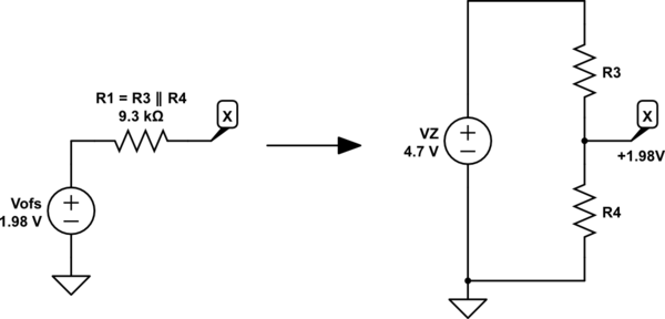
schematic

simulate this circuit

As per Thevenin's theorem, the parallel combination of R3 and R4 need to equal 9.3kΩ, and the potential at their junction should be +1.98V. These conditions give us two equations to be solved, to find R3 and R4:

$$ 4.7\frac{R_4}{R_3+R_4} = 1.98 $$

$$ \frac{R_3 R_4}{R_3 + R_4} = 9300 $$

I won't show my working here, just the solution:

$$ R_3 = 22k\Omega $$ $$ R_4 = 16k\Omega $$

Here's the final working circuit:
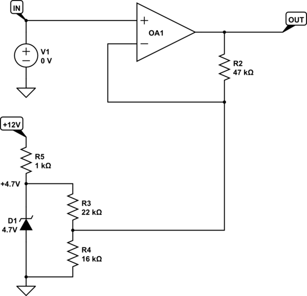
schematic

simulate this circuit
enter image description here

\$\endgroup\$
2
  • 1
    \$\begingroup\$ your mastering of the markup to get beautifully looking and easily readable formulas deserves +1 alone \$\endgroup\$
    – Maple
    Commented Jun 11, 2023 at 5:52
  • \$\begingroup\$ Thank you @Maple, your kind words are appreciated! \$\endgroup\$ Commented Jun 11, 2023 at 12:45
2
\$\begingroup\$

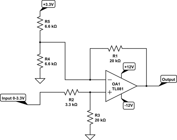
You need the reference to have the correct impedance. And if you want 0 V in to translate to -10 V output and 3.3V in to translate to +10 V output you need to feed the signal into the non-inverting input. Assuming you have 3.3 V available (either from the PWM circuit or a voltage reference IC) you can do that with a circuit like this:

schematic

simulate this circuit – Schematic created using CircuitLab
R1 and R3 should be equal while R4 || R5 should equal R2. (Actually the ratios just have to be the same, but it's easier to just use the same values)

Non-inverting gain: $$ A_V = 1+ \frac{R1}{R4 \parallel R5} = 1+\frac{20k}{3.3k} = 7.\overline{06} $$

Input signal attenuation: $$ {V_{in}}' = V_{in} \times \frac{R3}{R2 + R3} = V_{in} \times \frac{20k}{23.3k} = V{in}\times 0.858369 $$ For \$V_{in}\$ of 0 to 3.3 V, that makes the range \$0\$ to \$3.3\times 0.858369 \times 7.\overline{06} = 20V \$

Now you need that to be offset by -10 V.

Inverting gain: $$ A_V = -\left(\frac{R1}{R4 \parallel R5}\right) = -\left(\frac{20k}{3.3k}\right) = -6.\overline{06} $$ That will make the references contribution to the output \$6.\overline{06} \times3.3V / 2 = -10V\$ and your output range -10V to +10V.

If you don't have 3.3 V available for the reference you can use a different voltagee, such as 12 V, but you have to use a divider whose resistors in parallel are equal to the input resistor R2. The key to the whole thing is the R2 R3 voltage divider on the non-inverting input being the same ratio as the feedback and inverting input resistors.

\$\endgroup\$
2
  • 1
    \$\begingroup\$ Okay, I'll put that circuit into LTSpice and experiment with it and see how it goes. But the feedback resistor R1 is at the reference voltage path, not the signal path, what is the logic behind this? What I understand from what you said is that I need to match the input impedances with same resistors, but I want to put potentiometers somewhere to fine adjust the offset and the gain of the whole circuit, I need 1.65V(%50) PWM in the input to be more or less perfectly centered and be 0V DC at the output. If I put potentiometers, the input impedance matching would be broken, am I right? \$\endgroup\$ Commented Jun 10, 2023 at 21:12
  • \$\begingroup\$ @ÖmerGezer The ref voltage is going to the inverting input because it's being subtracted from the signal voltage. You can use pots to fine tune it, but with 1% resistors and a good op-amp it should be close. The small amount you'd have to change the impedances shouldn't matter. Using 3.3V reference the divider values are 2X the input resistor value so you can use the same value but put two in series for each leg of the divider, for example the 3.3k is a standard value, to get 6.6k in the divider put two 3.3k resistors in series. This way you only need two different resistor values. \$\endgroup\$
    – GodJihyo
    Commented Jun 11, 2023 at 15:12
2
\$\begingroup\$

First of all, you're trying to "amplify" a DIGITAL signal using an analog technique or an analog amplifier circuit; PWM is either high or low with no values in between.
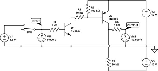
What's needed in your case is a simple "level-shifter" which can be made with two transistors, as below, for example:

schematic

simulate this circuit – Schematic created using CircuitLab

INPUT LOW (0V):
The transistor Q1 is off when the input is 0V or below 0.6V.
That keeps Q2 off and the output is pulled to -10V via R4 resistor.

INPUT HIGH (3.3V):
Q1 is on, which turns the Q2 on and connects the output to the +10V side.
The output is in phase with the input.

If you want this done with an op-amp, here is an example:

schematic

simulate this circuit

First, to clarify how an op-amp works:

  • It amplifies the difference between the non-inverting (+) and inverting (-) inputs, typically by about 100,000 times (depends on the specific model).
  • If the (+) input is higher than the (-) input even by 1mV, the output will be amplified 100,000 times or 100,000 times larger, that is +100,000mV or 100V.
  • Since most op-amps work at lower voltages, the output will be saturated, that is, it will go to the maximum positive value which is no more than its positive supply voltage.
  • If the (+) input is lower (more negative) than the (-) input (or the (-) input is higher or more positive than the (+) input) even by 1mV, the output will be amplified 100,000 times to 100V, but again it will only lead to saturation in the negative voltage direction.

Now to explain how this circuit works:

  • The inverting (-) input is set to one diode voltage drop of around 0.5V above ground (common).
  • Whenever the non-inverting (+) input goes below 0.5V, the output will go into negative saturation (close to negative supply voltage of the op-amp).
  • Whenever the non-inverting (+) input goes above 0.5V, the output will go into positive saturation (close to positive supply voltage of the op-amp).
  • 1k resistors at the input and the output limit the input and output currents in case of faults or overloads.
  • R4 resistor at the input merely keeps the input grounded in case of a disconnect from the signal source.
  • D1 can be replaced with a RED LED to give you about half of the 3.3V input signal voltage.
  • If you want to make it an inverting circuit, you merely swap the op-amp inputs.
  • Op-amp in this case works as a comparator instead of an amplifier.

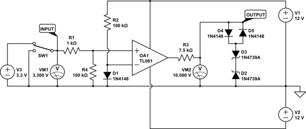
Here is another op-amp comparator but with voltage swing limited by output diodes:

schematic

simulate this circuit

\$\endgroup\$
6
  • \$\begingroup\$ Yes indeed, but with the only level shifters I know(like the adafruit bi-directional ones), I didn't know a way to scale the signal to -10V/+10V. A suitable shifter is a more elegant solution but I wanted to experiment with op-amps also. \$\endgroup\$ Commented Jun 10, 2023 at 20:45
  • \$\begingroup\$ I have added an op-amp circuit that does the same as the transistor circuit. I had started it hours ago, but had been busy, so I have just finished it now. I am working on an amplifier version of the circuit now (third example). Will let you know when it's done. \$\endgroup\$ Commented Jun 10, 2023 at 22:02
  • 1
    \$\begingroup\$ okay, the op-amp comparator circuit sure looks interesting and your explanation is clear, but it looks like I need to adjust the supply rail voltages precisely to match the op-amp saturation voltage to +-10 volts, am I right? For that I need to adjust the power supply and it's not an option in my case. By using op-amp amplifier configuration, I thought I would be able to carefully adjust the gain and the offset to set the output range exactly at -10V/+10V without touching the supply. \$\endgroup\$ Commented Jun 10, 2023 at 22:17
  • \$\begingroup\$ A comparator should work faster and is easier to make in cases like this one. Your op-amp supply voltage can remain higher and you can limit the output voltage range by other means like zeners with resistors in series. Most op-amps can't swing all the way up to the positive supply rail, many can't even reach the negative rail, which means your +12V will be more likely +10.5V at the output, depends on the op-amp model. \$\endgroup\$ Commented Jun 10, 2023 at 22:24
  • \$\begingroup\$ @ÖmerGezer I have added one more circuit, limiting the output voltages by using zener and standard diodes. \$\endgroup\$ Commented Jun 10, 2023 at 22:58
0
\$\begingroup\$

I don't know if this is a proper solution, but I guess I'll use this. Using the same circuit I posted in the original question, I just tinkered with the resistor values to have the intended offset and gain.

R3 and R2 represents a 10k potentiometer, to adjust the offset. R5 and R1 represents another 10k potentiometer, to adjust gain. So the weird values in the resistors are actually achievable.

The potentiometer adjustment is required in my application because %50 PWM input needs to exactly be 0V at the output(within small tolerances), and I intend to calibrate it before deployment.

The zener circuit next to the R3/R2 is needed in my application because the 12V rails are not stable, and can drift between 11.5V-13V.

Still not sure if there is something fundamentally wrong with using this op-amp circuit, since one of you pointed out in the answers that reference impedances should match, a concept I wasn't able to fully grasp and apply to my potentiometer adjustable circuit. But the simulation shows I get what I wanted with this crooked setup. However, please add any comments on what can go horribly wrong using this.

enter image description here

\$\endgroup\$

Your Answer

By clicking “Post Your Answer”, you agree to our terms of service and acknowledge you have read our privacy policy.

Not the answer you're looking for? Browse other questions tagged or ask your own question.