1
\$\begingroup\$

Relevant TI forum post with no resolution: here.

I am using an AOZ2264NQI-11 chip to convert 24 V down to 12 V. I originally designed this circuit for use with an AOZ2261NQI-12 chip, which has an identical footprint/pinout and a mostly identical application circuit (for more info read my previous question). I switched to the new chip to get the higher current output capability, 15 A vs 8 A.

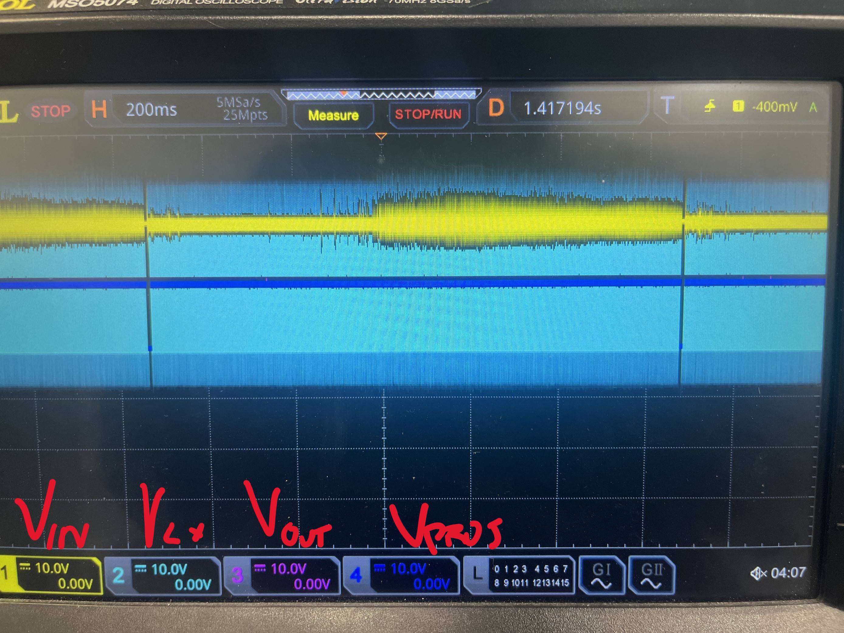
The problem I am seeing - or rather, hearing - is that once the load reaches ~2.5-3 A, the circuit begins to make an audible clicking noise. The noise is relatively loud and occurs roughly every 1.2 seconds, although it becomes more frequent as a higher load is applied. By the time the load hits ~8 A, the noise is frequent enough to be more of a hum. I haven't captured that behavior yet so I couldn't give a frequency but I am working on it.

When I first tested these PCBs with the lower-current chip, I also experienced the clicking but much less often. It would sometimes occur at a load of between 5.5-6 A, with roughly the same frequency.

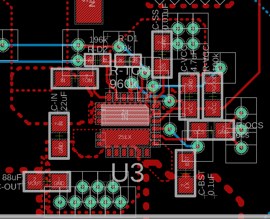
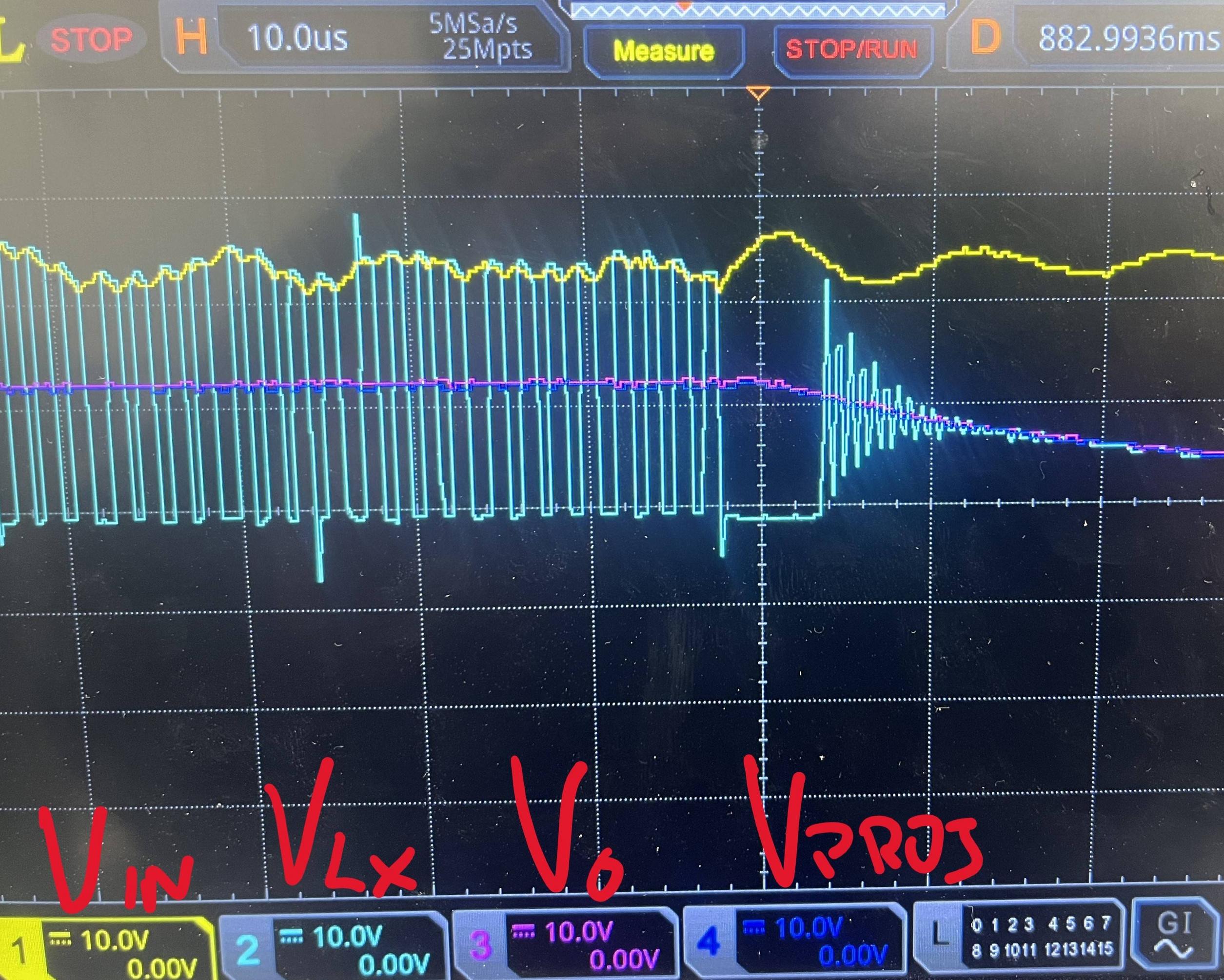
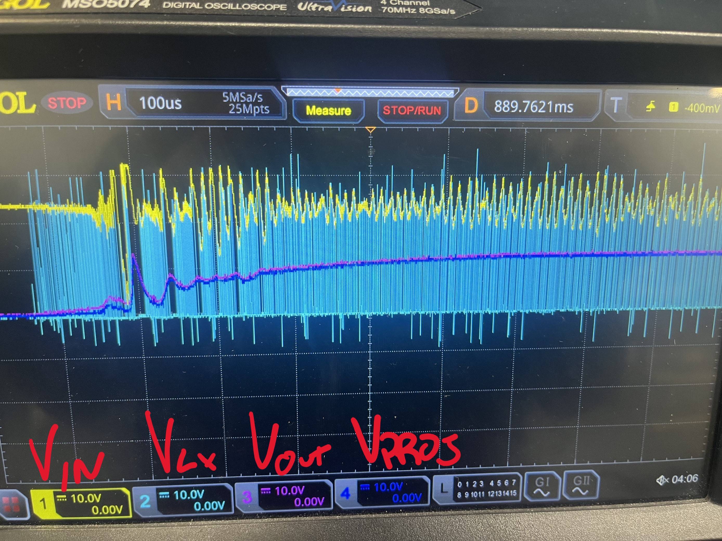
I am including the schematic, layout, and captures of relevant voltages when clicking: VIN, VLX, VOUT, and VPROJ, which is just the load voltage and differs from VOUT because there is a 0.03 Ω current sensing resistor in line with the load. Note: I am using a 100 kΩ resistor for ROCS, not the 20 kΩ value in the EDA snips.

Schematic

Layout

Clicking Zoomed Out

Clicking Start

Output Resuming

My next step is to examine the EN, PGOOD, and BST lines, and try to capture the clicking frequency at higher loads. I suppose I have two main questions:

  1. What buck regulator shutdown behavior causes an audible clicking? I don't believe it is thermal shutdown, using an IR gun the chip package sits at around 33°C even at higher loads.
  2. Why would the higher-current chip have this behavior at a lower load than the other chip? Apart from the ROCS value, the passive calculations are identical.
\$\endgroup\$
16
  • \$\begingroup\$ Not having the 0 volt reference markers on the oscilloscope pictures makes them fairly meaningless in my opinion. Where is VIN and VPROJ in your schematic. BTW the input voltage ripple looks really bad. \$\endgroup\$
    – Andy aka
    Commented Feb 14 at 21:01
  • \$\begingroup\$ @Andyaka fair points. 0V is the line that Vlx dips just below. Vin is IN in the schematic and Vproj isn't pictured in the schematic snippet. Vout is routed to one side of a 0.03ohm resistor, the other side goes directly into the load - that is Vproj. I could definitely have made those all clearer and more consistent. \$\endgroup\$
    – InBedded16
    Commented Feb 14 at 21:18
  • 2
    \$\begingroup\$ What size or part number is CIN? What happens if you put a 1000uF electrolytic in parallel? \$\endgroup\$ Commented Feb 14 at 22:41
  • 1
    \$\begingroup\$ 1 Mohm at the EN input could be critical. What else is connected at EN? \$\endgroup\$
    – Jens
    Commented Feb 14 at 23:24
  • 1
    \$\begingroup\$ The inductor choice looks good. However, what was the purpose of showing partial layout of your design then? You also don't show copper pours in your picture, so it is difficult to evaluate quality of high-current loops in your layout. To avoid problems, I would strongly recommend to start with manufacturer's recommended layout, and try to obtain reference designs and follow their BOM. \$\endgroup\$ Commented Feb 16 at 4:09

2 Answers 2

6
\$\begingroup\$

Ah, ceramic input capacitor strikes again.

...Most likely. I'll explain that a bit more, later. First, the capacitor itself:

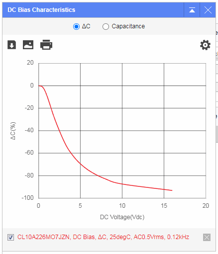
The AVX KGM15CR51C226MT does not have a datasheet (AVX provide sadly little data on their ceramic capacitors), but we can look up a comparable 22uF 16V 0603 X5R part, such as the Samsung CL10A226MO7JZN, which does:
https://weblib.samsungsem.com/mlcc/mlcc-ec.do?partNumber=CL10A226MO7JZN
enter image description here

You appear to be applying 24V which is unsafe for the 16V part anyway, but the dielectric and construction will not differ significantly from this part and we can assume there's a flea-fart's capacitance left at this voltage.

For a 10A class converter, I would expect more like 4-8 x 1206 or even 1210 chips, or a couple 0805s plus a polymer, and in either case an electrolytic would be welcome to absorb further ripple current plus dampen any input-circuit resonances.

Because type 2 ceramic capacitance depends on voltage, it's neither economical nor practical to select the largest possible value in a given voltage rating and chip size. Indeed, Digikey presently shows only three items of comparable rating, out of nearly a million items in the category; you selected quite the rare part.

More typical would be 4.7 to 22uF, 25 to 50V, 1206 or 1210, and such values will be available in X7R, which tends to have a flatter curve, also in terms of temperature (105°C rated).

As for function, SMPS controls typically assume a low and stable input impedance, or a stable input voltage. Clearly, neither of those are true here..!

There are two significant consequences for an under-damped input filter:

  1. Hot-plugging; inrush surge. This is a very common cause of failure among SMPS questions here (hence my comment).

    Even if the capacitor were linear, hot-plugging a voltage source to a lossless series LC circuit generates a peak voltage twice the input. Since C depends on V, as V rises, C decreases, dV/dt accelerates, V rises even further, C decreases even further... The resulting peak voltage can be five times the input, easily.

  2. Oscillation due to the converter's negative input impedance.

    That is, current draw decreases as voltage rises -- it conserves power more or less, so this is simply a natural consequence: negative (incremental) resistance. Depending on control type, this can manifest at frequencies as high as Fsw, or disappears above some fraction thereof (at frequencies where the control loop can't act fast enough to maintain constant input power), but in any case applies from DC up to some at least modest AC frequency which can include the input filter resonant frequency. Those frequencies overlap, the negative resistance exceeds loss resistance at that frequency, and off she sings.

So, simply dampening that with a bulk capacitor of nominal ESR, such as an electrolytic capacitor, keeps the regulator input happy. 100uF in polymer or electrolytic would be welcome, with more like 1000uF electrolytic being typical.

While it's true this may not be the explanation for the totality of observed behavior, including the clicking or bouncing or restarting, solving this is a prerequisite for further analysis.

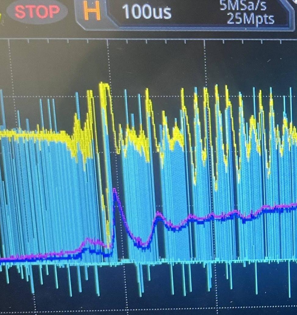
By the way, did you catch this juicy little bit? A closer look...
enter image description here

That peak looks suspiciously flat-topped, and if I'm not mistaken, that's a peak around 32V. On a device rated merely 28V... methinks you've observed avalanche breakdown, and are damn lucky the thing didn't fail shorted already!

24V is very tight to be operating a 28V converter at, anyway; I would advise keeping it under 20V, and using a TVS and electrolytic at the input, to dampen overshoot and ringing, and clamp overshoot to within the regulator's ratings. Else, get a higher-voltage rated regulator. Headroom around 40% (rated vs. nominal-max operating voltage) is recommended, give or take application.


Further reading: recently I simulated the transient, by itself as a startup (inrush) surge (not including the converter here), and collected a few related questions on the phenomena, in another answer:
https://electronics.stackexchange.com/a/713473/311631

\$\endgroup\$
4
  • 1
    \$\begingroup\$ Okay so it's going to take me a little time to work through your answer so I wanted to preempt that with a thank you, I appreciate it. I did think it was a little odd how sparse the recommended input (and output) filtering was in the datasheet, so I have a feeling you've nailed the issue. \$\endgroup\$
    – InBedded16
    Commented Feb 15 at 16:41
  • 1
    \$\begingroup\$ I agree with Tim's comments above. Fix the obvious problems first, it might be the solution. It will certainly help clear up some of the noise. If the problem persists, then at least you have a clean starting point to work from. \$\endgroup\$
    – John D
    Commented Feb 15 at 18:39
  • \$\begingroup\$ Okay so I've done some redesign here. Input filtering is now 2x 10uF 1206s, 2x 22uF 1206s, and a 390uF electrolytic. Output filtering is 4x 22uF 1206s. Voltage ratings are 50V when possible and 35V otherwise. It'll be another week or so before I can test it. \$\endgroup\$
    – InBedded16
    Commented Feb 19 at 18:11
  • 1
    \$\begingroup\$ Hey Tim Williams you're a genius! New boards are in and working better than I could have hoped for. I can pull 13.5A with noise of only +/- 0.5V, my only limitation now is heat dissipation. The clicking noise is also totally absent. Marking this as the answer, thank you very much! \$\endgroup\$
    – InBedded16
    Commented Mar 1 at 15:21
1
\$\begingroup\$

Just to illustrate the Tim Williams comment. Below is an example from TI part with embedded inductor. Please note the number and spectrum of capacitors on input and output: enter image description here You should practice something similar.

\$\endgroup\$

Your Answer

By clicking “Post Your Answer”, you agree to our terms of service and acknowledge you have read our privacy policy.

Not the answer you're looking for? Browse other questions tagged or ask your own question.