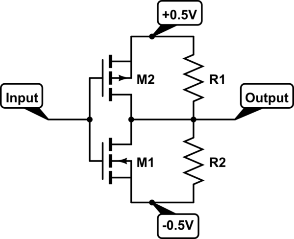
A PMOS over a NMOS would work as a ternary inverter if the supply voltage is low (slightly above the threshold voltage):

simulate this circuit – Schematic created using CircuitLab
At -0.5V input, the output will be raised by M2 to 0.5V.
At 0V input, both transistors will be "Off" and the resistors will pull the output back to 0V.
At 0.5V input, M2 will shut off and M1 will turn on pulling output to -0.5V.
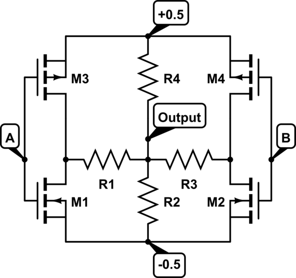
A Ternary NOR could be this:

Truth Table:
00 0
0+ -
0- +
+- 0
++ -
-- +
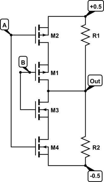
A Ternary NAND could be this:

Truth Table:
00 0
0+ 0
0- 0
+- 0
-- +
++ -
I would assume more complicated ternary gates could be made based on similar principles.
It's interesting to note that a major disadvantage of this topology is the loss of speed due to RC settling times where the C is inherent capacitance of the transistors. One possible advantage of this may be the required low-voltage and therefore low power draw of the circuits.
