I'm in the process of leaning to design pcb's and leaning to solder tiny QFN parts. As part of this process, I'm trying to create a circuit with the TPS63001 (datasheet: http://www.ti.com/lit/ds/symlink/tps63001.pdf) buck-boost converter, which I would like to use to power a ESP8266 (which requires 3.3v) by a lipo.
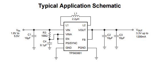
According to the datasheet, the circuit should be:

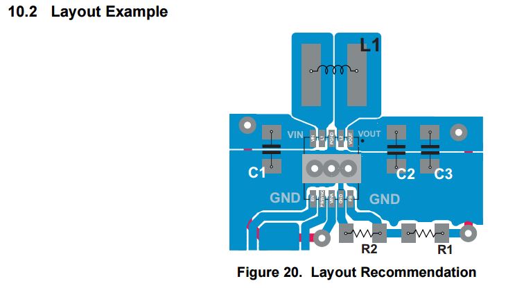
And in the same datasheet, they even provide a layout example:

This layout is for the Adjustable Output Voltage version, I will be using the fixed voltage version.
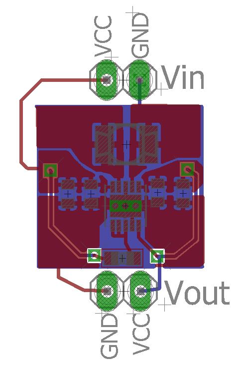
With the information in the datasheet, I created this layout in eagle:

Now there are a few things I'm wondering:
- There are three dots underneath the chip in the example in the datasheet. I guessed that these would be via's, and created a ground plane on the back of the board. I guess this is for heat dispensation, did I interpret this right?
- I connected VINA, EN and PS/SYNC together. In the layout example EN and VINA just move out of the picture, but according to the schema, they should be connected, did I do this right?
Are there any other dising rules / recommendations that I should take care of?
