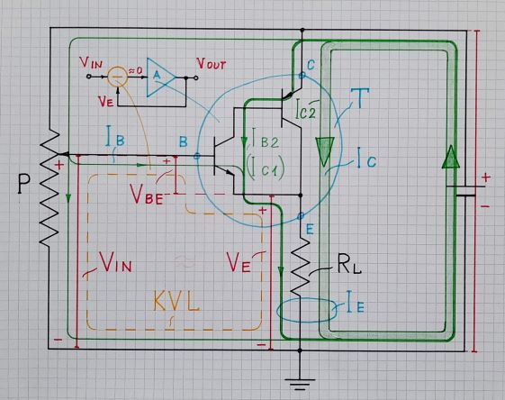
I have illustrated much of what was said in the answers and comments above and expanded it by some of my thoughts.
1. Compound transistor. The n-p-n and p-n-p transistor connected in this way form a compound n-p-n transistor T (in blue). We can think of this combination of as a "weak" n-p-n transistor "helped" by a stronger "brother" or, in terms of equivalent electrical circuits, as of two current sources in parallel. With a little more imagination, it can reminds the Howland current pump where another "helping" current source is connected in parallel to the the imperfect input current source... like an INIC negative resistor...
2. "Emitter" follower. Once accepted it is just a single transistor, we see that here it is connected in the well-known circuit of an emitter follower. It copies, by means of the negative feedback principle (the little block diagram), the input voltage VIN on the load RL as follows:
The output voltage VE is compared with the input voltage in the possibly simplest way - by connecting the two voltage sources contrary in series. So their voltages are subtracted according to KVL... and the result is applied to the amp input (the base-emitter junction). Note the compared voltages are grounded while the input, where the result appears, is floating. Thus the subtractor (in yellow in the block diagram) is made at no cost; it is just the loop... a piece of wire...
When we change the input voltage VIN by moving the potentiometer slider, the Sziklai transistor T reacts to this "input disturbance". It begins increasing its "emitter" current through the load RL and, accordingly, the output voltage VE across it, until reaches the equilibrium (with VBE below VIN). This is, roughly outlined, the mechanism of this kind of negative feedback called "emitter degeneration".
3. Active diode. Now let's try to see another (internal) negative feedback. Remember the so-called "active diode" that exploits a dual kind of negative feedback. There the output (collector-emitter part) is connected in parallel to the input (base-emitter junction); this is simply a transistor which collector is connected to the base.
So we can note that in the Sziklai configuration, there is such a connection (negative feedback network) between the collector and base of the output transistor... and this is the collector-emitter part of the first transistor. It turns out that when the input transistor is close to saturation, it will act as a feedback network (like a piece of wire) that conveys the collector voltage variations to the base. As a result of this negative feedback, the output transistor will be never saturated (will be ever in active mode).
Of course, in this emitter follower application, the input transistor is never saturated... but in other applications where its emitter is firmly connected to fixed voltage (common-emitter stage), it can be saturated...

