I am doing a PCB layout with a Atmel/Microchip MCU ATSAML21E18B-MUT which has QFN-32 package 5x5 mm. This board can have a maximum of 20x40 mm and I am having problems with space because the circuit is not very little and also there is an NFC antenna on-board that occupies 14x14 mm on both sides.
The drawing of "32 pin QFN" is on page 1123. The datasheet does not mention if this pad should or not be connected to GND or other signal.
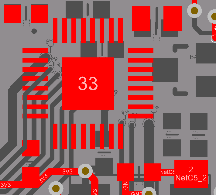
Check my current drawing of QFN-32 package on the current layout below, there is a 2.8x2.8 mm square pad in the center, also known as an exposed pad. I want to delete it... in order I can route tracks and vias below the QFN package. Doing this I would finish the layout easily.
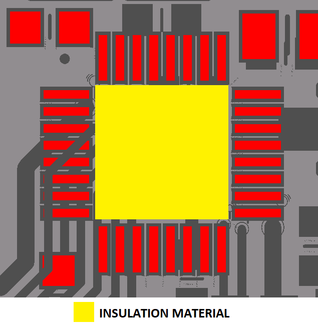
And, when assembling the boards, I want to place an electrical insulation material between the IC package and the board, to guarantee there will be no short-circuit between the center pad of the QFN-32 package and a via or track, for example, if the solder mask doesn't guarantee it.
Then, in this case, can I securely remove the center pad of the QFN-32 from the PCB layout?
- OBS1: It is a double-side board, there is no possibility to go multilayer.
- OBS2: The IC does not heat.
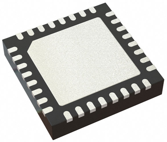
The package:


