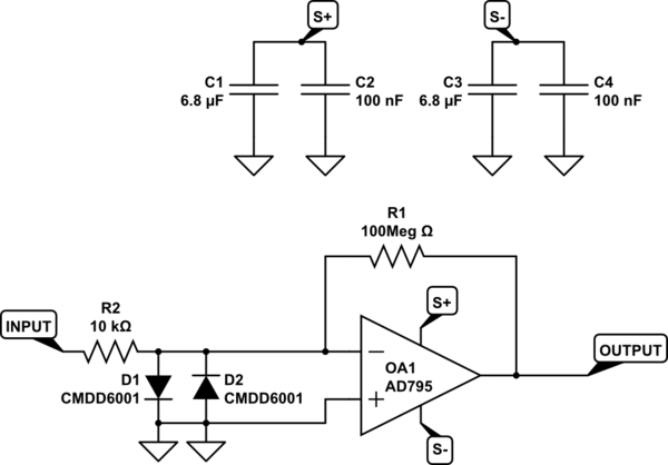
I'm trying to build a trans-impedance amplifier shown in the circuit below. However, with my op-amp of choice, the AD795, I'm a bit confused by their circuit board notes and how to implement them. The input node sends a current in pico-amp range, and the TIA converts it into a voltage at the output. Considering how tiny the input is, it's very critical to maintain the pico-Amp resolution at the input. Looking at the datasheet, it shows some notes about this.

simulate this circuit – Schematic created using CircuitLab
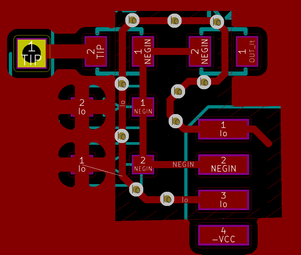
The first thing they mention is a guard ring in figure 34. Using the unconnected pin pad 1, I can connect it to the bias and draw a guard trace around the input signal path in a no-copper-pour zone so all there is is the signal trace and the guard ring. I can add vias within the ring, as evidenced by what Analog Devices did with this evaluation board for the ADA4350. Below is a rough concept of how I envision implementing the guard ring.
However, in the next section at Figure 36, the datasheet mentions how leakage could still occur, and they recommend that I could bend up the input pin and solder it to a teflon-insulated standoff. I'm confused as to how it fits in with all of the other recommendations. From the looks of it, doing so would leave the pin hanging in the air, making the guard trace/via fence worthless. Soldering it directly to a standoff like this doesn't allow for a way to directly connect to the circuit board without using a wire to connect to another pad.
Seeing the dilemma with these protection techniques, how are they implemented in practice? Are the two ideas mutually exclusive, or can they work together?

