I have been looking over multiple designs for ideal diodes using FET transistors such as the circuits from these posts:
Understanding an 'ideal' diode made from a p-channel MOSFET and PNP transistors
and from this site:
http://jiggerjuice.info/electronics/projects/power/ideal-diode.html
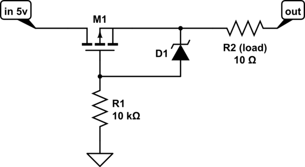
The part that I don't understand is why they use so many other components in their designs. My question is if the following circuit I designed functions the same as the ones linked above.

simulate this circuit – Schematic created using CircuitLab
The zener diode is being used to protect the gate terminal on the FET.
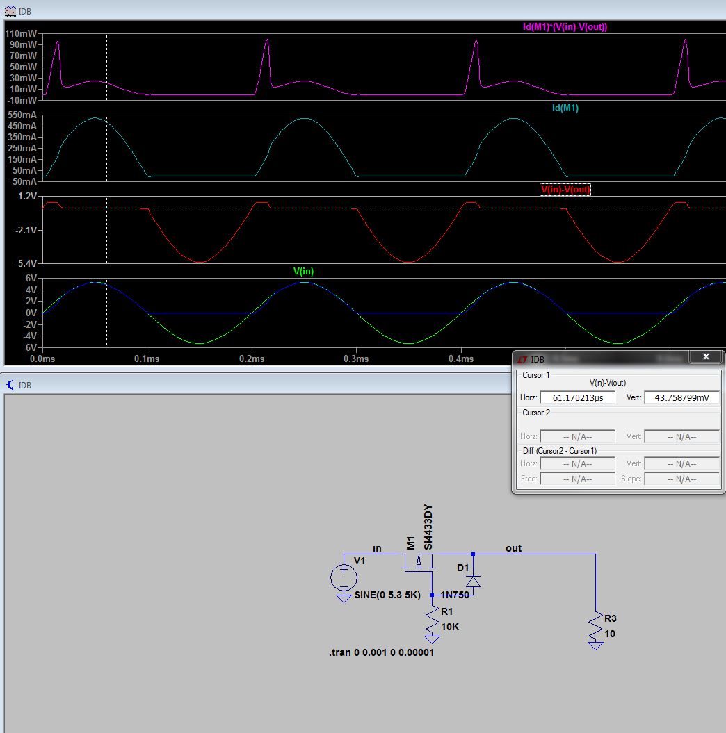
edit: for use as a high side half wave rectifier:

