Tweeted twitter.com/StackElectronix/status/1009945285446062081
added 450 characters in body
Source Link
Geo
  • 754
  • 8
  • 21

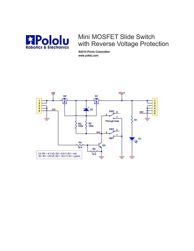
I would like to incorporate this circuit in my design so that I could use a low current capacity slide switch to control the 2A current of a Li-poly.

Now, I understand the purpose of having two PMOS for bidirectional current control as discussed here and the purpose of the zener diode D2 for clamping the gate voltage to a voltage below the maximum allowable voltage of the gate as discussed here.

Finally, the BJT Q3 allows for controlling the gates of the two PMOS through a GPIO pin.

But what is the purpose of R3 in this circuit? (Can it be ommited?)

reverse voltage protection circuit

EDIT: Of course, how did I not see that from the start? To be honest it seemed strange to me that R3 was pulled up to the path between Q1 and Q2 rather that to Vin , but now I understand that it is only between Q1,Q2 that one can be sure there is a path to the supply, since the circuit works biderectionally (i.e if voltage was applied from Vout and R3 was pulled up to Vin, the top end of R3 would be floating).

Thanks for the replies

I would like to incorporate this circuit in my design so that I could use a low current capacity slide switch to control the 2A current of a Li-poly.

Now, I understand the purpose of having two PMOS for bidirectional current control as discussed here and the purpose of the zener diode D2 for clamping the gate voltage to a voltage below the maximum allowable voltage of the gate as discussed here.

Finally, the BJT Q3 allows for controlling the gates of the two PMOS through a GPIO pin.

But what is the purpose of R3 in this circuit? (Can it be ommited?)

reverse voltage protection circuit

EDIT: Of course, how did I not see that from the start? To be honest it seemed strange to me that R3 was pulled up to the path between Q1 and Q2 rather that to Vin , but now I understand that it is only between Q1,Q2 that one can be sure there is a path to the supply, since the circuit works biderectionally (i.e if voltage was applied from Vout and R3 was pulled up to Vin, the top end of R3 would be floating).

Thanks for the replies
Source Link
Geo
  • 754
  • 8
  • 21

Is this resistor necessary for protection?

I would like to incorporate this circuit in my design so that I could use a low current capacity slide switch to control the 2A current of a Li-poly.

Now, I understand the purpose of having two PMOS for bidirectional current control as discussed here and the purpose of the zener diode D2 for clamping the gate voltage to a voltage below the maximum allowable voltage of the gate as discussed here.

Finally, the BJT Q3 allows for controlling the gates of the two PMOS through a GPIO pin.

But what is the purpose of R3 in this circuit? (Can it be ommited?)

reverse voltage protection circuit