deleted 43 characters in body
Source Link
Voltage Spike
  • 88.8k
  • 49
  • 90
  • 234

I am a beginner and I am trying to understand the block diagram of a Static RAM. I want to draw a "256x4 bit SRAM" block diagram. According to some information I collected from the internet I managed to draw a block diagram for a "256x8 bit SRAM" which is demonstrated in the following figure (I am not sure if it is correct): enter image description here
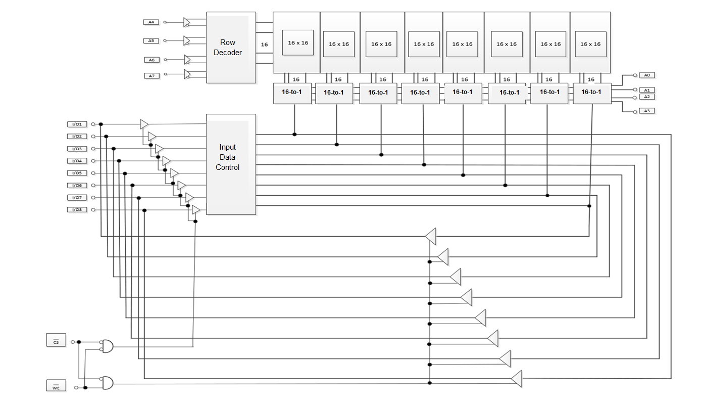
However,I am a bit confused with the way it works. Could you provide an example about reading or writing data? Which signals are activated, which switches and which gates open and close?

In addition to this, what does determine the number of bits I use for the input of the Row Decoder? I know that for n bits in the input we get 2^n bits in the output of the decoder. So here I get 16 bits. But why do I have 4 bits in the input (A4,A5,A6,A7). Any help is appreciated. Thanks in advance!

I am a beginner and I am trying to understand the block diagram of a Static RAM. I want to draw a "256x4 bit SRAM" block diagram. According to some information I collected from the internet I managed to draw a block diagram for a "256x8 bit SRAM" which is demonstrated in the following figure (I am not sure if it is correct): enter image description here

However,I am a bit confused with the way it works. Could you provide an example about reading or writing data? Which signals are activated, which switches and which gates open and close?

In addition to this, what does determine the number of bits I use for the input of the Row Decoder? I know that for n bits in the input we get 2^n bits in the output of the decoder. So here I get 16 bits. But why do I have 4 bits in the input (A4,A5,A6,A7).

Source Link
MJ13
  • 249
  • 1
  • 3
  • 10

SRAM-Logic Block Diagram

I am a beginner and I am trying to understand the block diagram of a Static RAM. I want to draw a "256x4 bit SRAM" block diagram. According to some information I collected from the internet I managed to draw a block diagram for a "256x8 bit SRAM" which is demonstrated in the following figure (I am not sure if it is correct): enter image description here

However,I am a bit confused with the way it works. Could you provide an example about reading or writing data? Which signals are activated, which switches and which gates open and close?

In addition to this, what does determine the number of bits I use for the input of the Row Decoder? I know that for n bits in the input we get 2^n bits in the output of the decoder. So here I get 16 bits. But why do I have 4 bits in the input (A4,A5,A6,A7). Any help is appreciated. Thanks in advance!