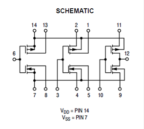
The schematic below is of a CD4007 mosMOS transistor chip.
From the schematic it can be seen that on either side, pmosPMOS or nmosNMOS, the arrows indicating what type of mosMOS transistor it is, are all connected to a single pin, - pin 7 for the nmosNMOS side, and pin 14 on the pmosPMOS side. In this case, pin 7 is a source and pin 14 is a drain.
Why is that? Does anything need to be connected to those pins to use the other transistor in the chip?

