added 212 characters in body
Source Link

I have some questions concerning this schematic:

enter image description hereupdated sch for psu of gate drv

What is the topology used here? I am guessing flyback without feedback circuitry.

Why is the TPS40211 utilized here? Is it to provide more current? Rather than using the 15 V of the input, this chip is used to provide more current for the tl494 which in turn will power the gate drivers to drive the IGBTs (which require +4 A). Am I right?

The transformer has two identical secondaries. Each one is used to drive the output of a gate driver, which requires a bi-bolar power supply. How can I use each secondary to provide both +15 V and -15 V?

There is a note in the gate driver transformer datasheetdatasheet: "These gate drive transformers are meant to operate between 50 and 300 kHz with a 12 V, 45% bipolar waveform". Does that mean it can't operate at 15 V?

The circuits are basically the same as the typical recommendation in the datasheet but I couldn't figure out the connection between the two ICs.

The circuit goes something like this:

enter image description here

I have some questions concerning this schematic:

enter image description here

What is the topology used here? I am guessing flyback without feedback circuitry.

Why is the TPS40211 utilized here? Is it to provide more current? Rather than using the 15 V of the input, this chip is used to provide more current for the gate drivers to drive the IGBTs (which require +4 A). Am I right?

The transformer has two identical secondaries. Each one is used to drive the output of a gate driver, which requires a bi-bolar power supply. How can I use each secondary to provide both +15 V and -15 V?

There is a note in the gate driver transformer datasheet: "These gate drive transformers are meant to operate between 50 and 300 kHz with a 12 V, 45% bipolar waveform". Does that mean it can't operate at 15 V?

The circuits are basically the same as the typical recommendation in the datasheet but I couldn't figure out the connection between the two ICs.

The circuit goes something like this:

enter image description here

I have some questions concerning this schematic:

updated sch for psu of gate drv

What is the topology used here? I am guessing flyback without feedback circuitry.

Why is the TPS40211 utilized here? Is it to provide more current? Rather than using the 15 V of the input, this chip is used to provide more current for the tl494 which in turn will power the gate drivers to drive the IGBTs (which require +4 A). Am I right?

The transformer has two identical secondaries. Each one is used to drive the output of a gate driver, which requires a bi-bolar power supply. How can I use each secondary to provide both +15 V and -15 V?

There is a note in the gate driver transformer datasheet: "These gate drive transformers are meant to operate between 50 and 300 kHz with a 12 V, 45% bipolar waveform". Does that mean it can't operate at 15 V?

The circuits are basically the same as the typical recommendation in the datasheet but I couldn't figure out the connection between the two ICs.

The circuit goes something like this:

enter image description here

added 50 characters in body; edited title
Source Link
ocrdu
  • 9.3k
  • 23
  • 32
  • 42

what What is the most used bi-polar output SMPS topology in gate driver isolation?

I have some questions concerning the attachedthis schematic.:

enter image description here

What is the topology used here? I am guessing flyback without feedback circuitry!.

Why is the TPS40211TPS40211 utilized here? isIs it to provide more current? Rather than using the 15V15 V of the input, this chip is used to provide more current for the gate drivers to drive the IGBTs (require +4Awhich require +4 A). amAm I right?

The transformer has 2two identical secondaries each. Each one is used to drive the output of a gate driver, which requirerequires a bi-bolar power supply how. How can I use each secondary to provide both +15V+15 V and -15V15 V?

There is a note in the Gategate driver transformer datasheet: 'These"These gate drive transformers are meant to operate between 50 and 300 kHz with a 12V12 V, 45% bipolar waveform'waveform". Does that mean it can't operate at 15V15 V?

The circuits are basically the same as the typical recommendation in datasheetsthe datasheet but I couldn't figure out the connection between the 2two ICs.

enter image description here

The circuit goes something like this: enter image description here

Thank you,enter image description here

what is the most used bi-polar output SMPS topology in gate driver isolation?

I have some questions concerning the attached schematic.

What is the topology used here? I am guessing flyback without feedback circuitry!

Why is the TPS40211 utilized here? is it to provide more current? Rather than using the 15V of the input this chip is used to provide more current for the gate drivers to drive the IGBTs (require +4A). am I right?

The transformer has 2 identical secondaries each one is used to drive the output of a gate driver, which require a bi-bolar power supply how can I use each secondary to provide both +15V and -15V?

There is a note in the Gate driver transformer datasheet: 'These gate drive transformers are meant to operate between 50 and 300 kHz with a 12V, 45% bipolar waveform'. Does that mean it can't operate at 15V?

The circuits are basically the same as the typical recommendation in datasheets but I couldn't figure out the connection between the 2 ICs.

enter image description here

The circuit goes something like this: enter image description here

Thank you,

What is the most used bi-polar output SMPS topology in gate driver isolation?

I have some questions concerning this schematic:

enter image description here

What is the topology used here? I am guessing flyback without feedback circuitry.

Why is the TPS40211 utilized here? Is it to provide more current? Rather than using the 15 V of the input, this chip is used to provide more current for the gate drivers to drive the IGBTs (which require +4 A). Am I right?

The transformer has two identical secondaries. Each one is used to drive the output of a gate driver, which requires a bi-bolar power supply. How can I use each secondary to provide both +15 V and -15 V?

There is a note in the gate driver transformer datasheet: "These gate drive transformers are meant to operate between 50 and 300 kHz with a 12 V, 45% bipolar waveform". Does that mean it can't operate at 15 V?

The circuits are basically the same as the typical recommendation in the datasheet but I couldn't figure out the connection between the two ICs.

The circuit goes something like this:
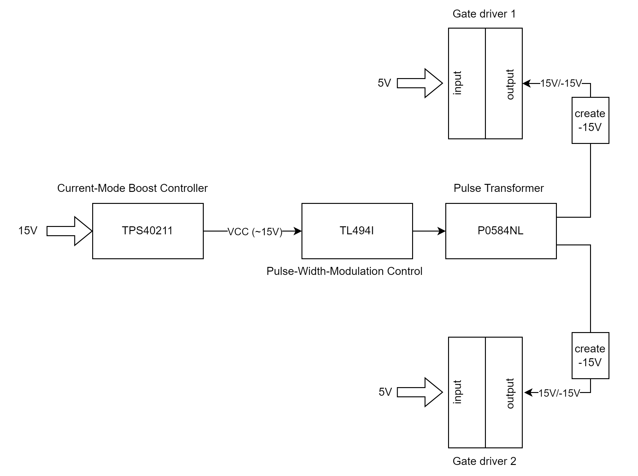
enter image description here

Source Link

what is the most used bi-polar output SMPS topology in gate driver isolation?

I have some questions concerning the attached schematic.

What is the topology used here? I am guessing flyback without feedback circuitry!

Why is the TPS40211 utilized here? is it to provide more current? Rather than using the 15V of the input this chip is used to provide more current for the gate drivers to drive the IGBTs (require +4A). am I right?

The transformer has 2 identical secondaries each one is used to drive the output of a gate driver, which require a bi-bolar power supply how can I use each secondary to provide both +15V and -15V?

There is a note in the Gate driver transformer datasheet: 'These gate drive transformers are meant to operate between 50 and 300 kHz with a 12V, 45% bipolar waveform'. Does that mean it can't operate at 15V?

The circuits are basically the same as the typical recommendation in datasheets but I couldn't figure out the connection between the 2 ICs.

enter image description here

The circuit goes something like this: enter image description here

Thank you,