deleted 46 characters in body
Source Link
Transistor
  • 180.5k
  • 14
  • 194
  • 417

enter image description here

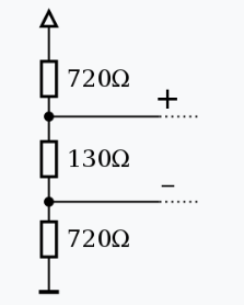
Figure 1. RS485 biasing network. Image by Stündle, Creative Commons. Note that both lines are biased positive and with the resistor values shown the + and - lines will be roughly 55% and 45% of supply voltage in the idle state.

From the same source:

enter image description here

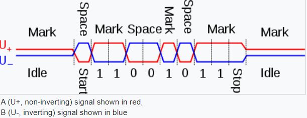
Figure 2. Switching of the RS485 signal.

USB will be similar.

Or is it a case of the negative of the diff pair could be 0 - 2 V and the positive line 2 - 4 V (with respect to the actual USB ground)?

Generally not. The two inputs will be fed into a comparator and what you really want is polarity inversion at the inputs for clear logic levels. That means the inputs should have a close-to common level for high and low levels and the drivers should flip between themThe signals are compared with each other rather than to an absolute reference.

enter image description here

Figure 1. RS485 biasing network. Image by Stündle, Creative Commons. Note that both lines are biased positive and with the resistor values shown the + and - lines will be roughly 55% and 45% of supply voltage in the idle state.

From the same source:

enter image description here

Figure 2. Switching of the RS485 signal.

USB will be similar.

Or is it a case of the negative of the diff pair could be 0 - 2 V and the positive line 2 - 4 V (with respect to the actual USB ground)?

Generally not. The two inputs will be fed into a comparator and what you really want is polarity inversion at the inputs for clear logic levels. That means the inputs should have a close-to common level for high and low levels and the drivers should flip between them.

enter image description here

Figure 1. RS485 biasing network. Image by Stündle, Creative Commons. Note that both lines are biased positive and with the resistor values shown the + and - lines will be roughly 55% and 45% of supply voltage in the idle state.

From the same source:

enter image description here

Figure 2. Switching of the RS485 signal.

USB will be similar.

Or is it a case of the negative of the diff pair could be 0 - 2 V and the positive line 2 - 4 V (with respect to the actual USB ground)?

Generally not. The two inputs will be fed into a comparator and what you really want is polarity inversion at the inputs for clear logic levels. The signals are compared with each other rather than to an absolute reference.
Source Link
Transistor
  • 180.5k
  • 14
  • 194
  • 417

enter image description here

Figure 1. RS485 biasing network. Image by Stündle, Creative Commons. Note that both lines are biased positive and with the resistor values shown the + and - lines will be roughly 55% and 45% of supply voltage in the idle state.

From the same source:

enter image description here

Figure 2. Switching of the RS485 signal.

USB will be similar.

Or is it a case of the negative of the diff pair could be 0 - 2 V and the positive line 2 - 4 V (with respect to the actual USB ground)?

Generally not. The two inputs will be fed into a comparator and what you really want is polarity inversion at the inputs for clear logic levels. That means the inputs should have a close-to common level for high and low levels and the drivers should flip between them.