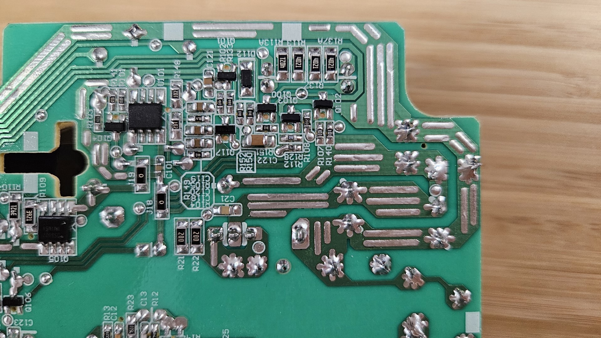
I recently took apart a DeWalt battery charger. What is the purpose of this particular arrangement of exposed copper on certain traces (mostly on the right side of the image)? These are wide, high-current traces, so naturally I assume this is for heat dissipation, but is there a reason for making such exposed areas in narrow, parallel lines? My intuition is that it allows two things: (1) a more controlled flow of paste in the oven, and (2) less paste overall for only slightly decreased thermal area. Is this correct?

