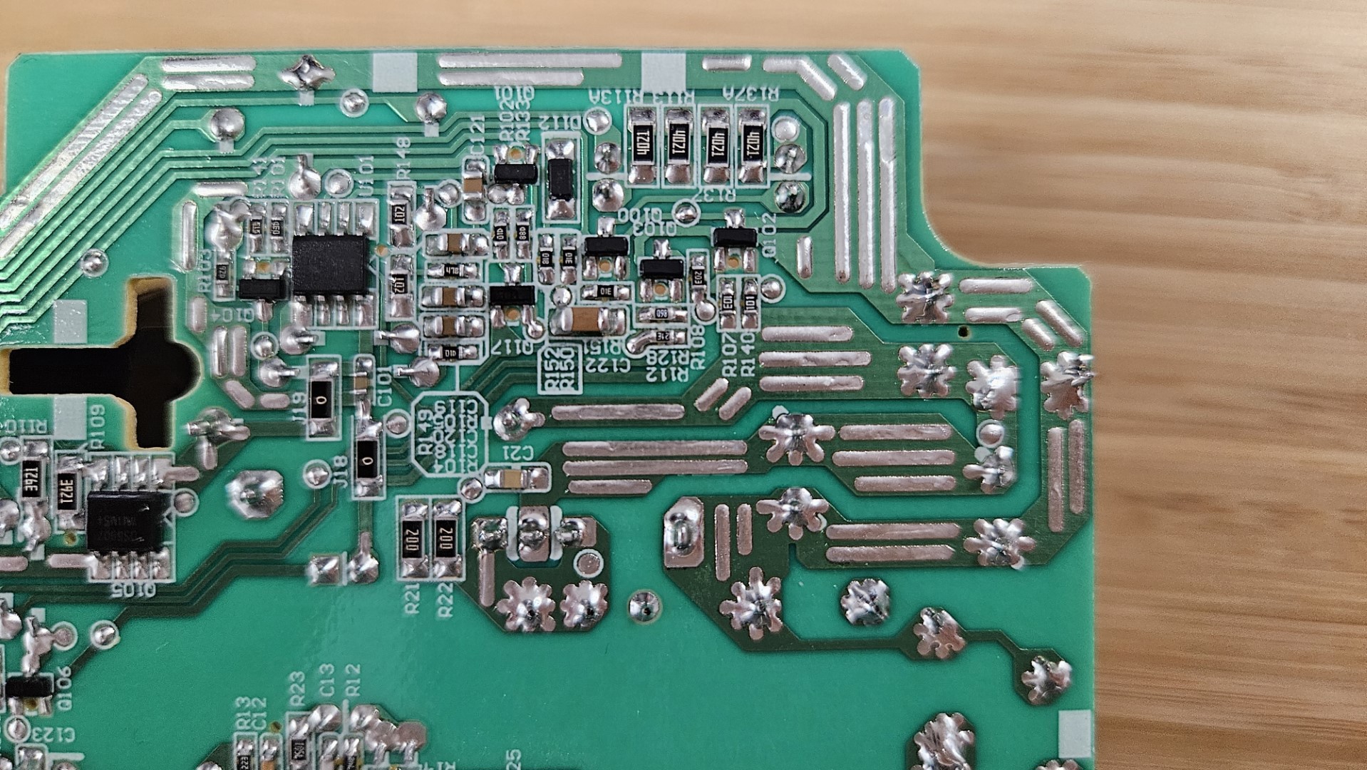
I recently took apart a DeWalt battery charger. What is the purpose of this particular arrangement of exposed copper on certain traces (mostly on the right side of the image)? These are wide, high-current traces, so naturally I assume this is for heat dissipation, but is there a reason for making such exposed areas in narrow, parallel lines? My intuition is that it allows two things: (1) a more controlled flow of paste in the oven, and (2) less paste overall for only slightly decreased thermal area. Is this correct?
2 Answers
This is commonly done in an attempt to increase the current handling capability of traces. You need to keep in mind that the copper on PCBs is only around 35µm thick (typically), so adding even just a very small amount of metal in the form of solder will improve things.
It's up for debate, of course, whether this is actually worth doing.
In case of the PCB you've shown, the trace on the top left ended up a little dry - it might've been better to interrupt the exposed areas with solder mask more frequently, which would've helped to retain more liquid solder during the wave soldering process.
Removing some solder mask is definitely cheaper than using a PCB with thicker copper, though.
Your intuition is right. If the areas were totally exposed (no solder mask) you could have tombstone effects on the components connected to these areas. See tombstone effect https://youtu.be/MaaOmI5gO08?si=jpHEvB1BMJ-uN-lO
This geometry and amount of exposed copper is a compromise for the manufacturing phase.
-
\$\begingroup\$ Were you perhaps thinking of thermal reliefs rather than the increased current capacity due to greater conductor cross-section that's relevant to the question? \$\endgroup\$ Commented Apr 8 at 17:59
-
\$\begingroup\$ Yes, I was talking about thermal reliefs. It seemed to me that the question was about the particular arrangement of exposed copper on certain traces = increasing thermal dissipation (that's what the OP was suggesting). \$\endgroup\$– VincentCommented Apr 8 at 19:20
-
5\$\begingroup\$ I'm not convinced that having exposed copper does anything for tombstoning. The thermal impedance of the soldermask is pretty insignificant. \$\endgroup\$– HearthCommented Apr 8 at 19:55
-
3\$\begingroup\$ The board in question is wave soldered, not reflowed. All SMD components are glued down and won't go anywhere no matter what. \$\endgroup\$ Commented Apr 8 at 23:44

