8
\$\begingroup\$

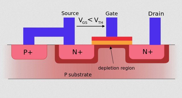
Wikipedia has several pictures of MOSFETs and various types of them. Here is one.

enter image description here

Notice that the Source and Body are connected. I understand this is to ensure there is no forward-bias or reverse-bias between them.

What I don't understand is, what is that "P+" region where the body connection exists? What is it and what is it's purpose? If it's a more highly-doped p-region then I don't understand why.

\$\endgroup\$

1 Answer 1

15
\$\begingroup\$

In a semiconductor, you can't generally make a resistive (ohmic) contact to a lightly doped region (as in the p substrate or bulk here). Such a contact would likely be very resistive, or act as a Schottky diode.

So (just like the N+ in the drain), a very heavy P+ diffusion is made for the metallic contact. This creates a degenerate (i.e. metallic or conductive) junction between the metal and the semiconductor, thus giving a good electrical contact to the bulk.

A secondary advantage of this is that the P+ bulk and N+ source can be quite close together. Having a low resistance connecting shorting these makes the FET more robust during high VDS voltages.

\$\endgroup\$
2
  • \$\begingroup\$ Thank you, this explains a lot. But a follow-up question, is the same thing required on the opposite mosfet? So an n-substrate and p-type channels, do you need an N+ region for the ohmic contact? \$\endgroup\$
    – DrZ214
    Commented Sep 5, 2021 at 22:18
  • 1
    \$\begingroup\$ Yes; you need a ++ contact for all lightly doped regions. \$\endgroup\$
    – jp314
    Commented Sep 6, 2021 at 0:22

Your Answer

By clicking “Post Your Answer”, you agree to our terms of service and acknowledge you have read our privacy policy.

Not the answer you're looking for? Browse other questions tagged or ask your own question.