3
\$\begingroup\$

enter image description here

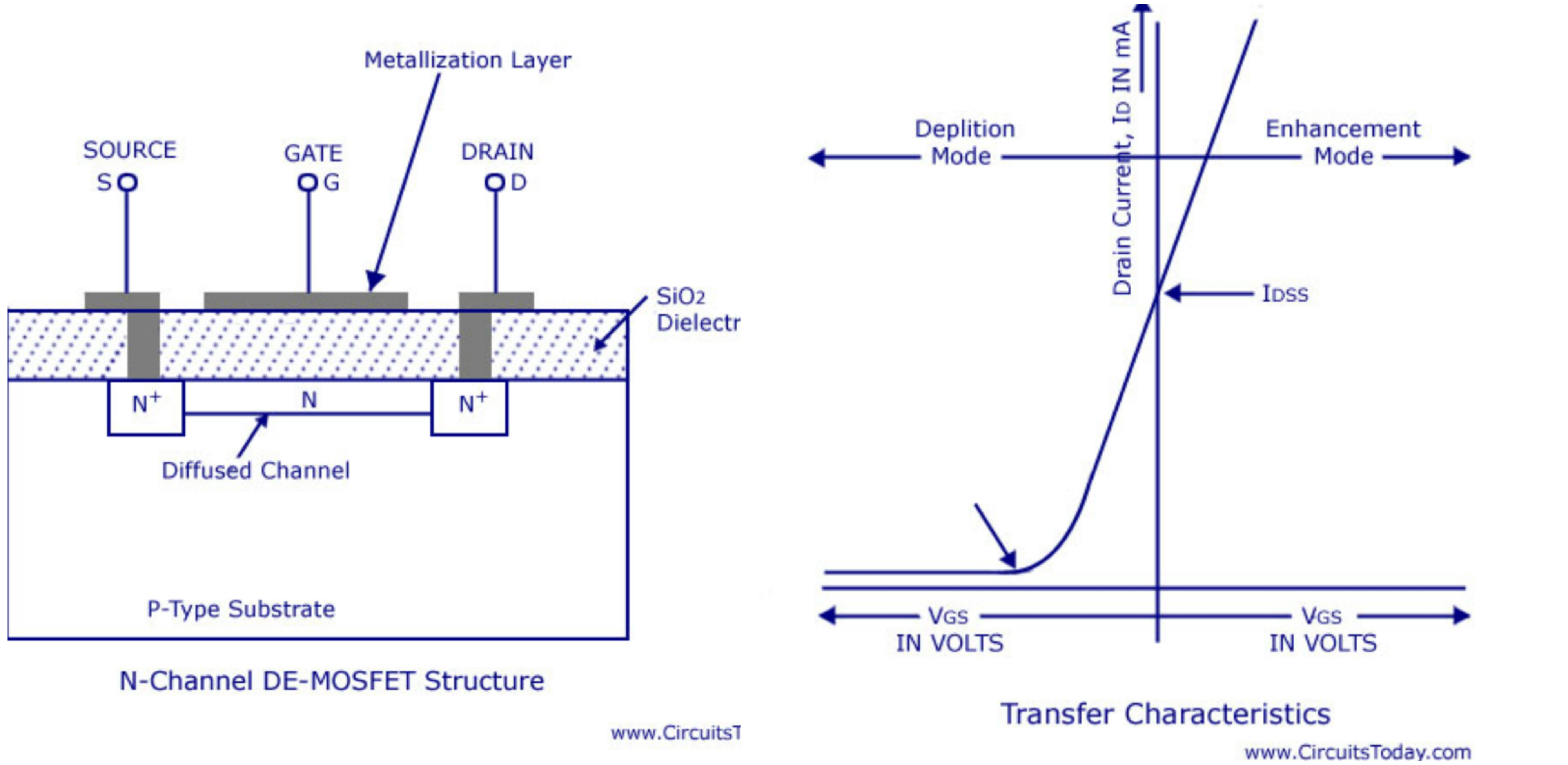
I'm trying to understand the working of an n-channel depletion type MOSFET. I'm confused why no tutorial talks about the depletion region between the P and N type silicon i.e between the 'bulk' and the 'channel'.

Even if I were to consider that the depletion region is actually present but neglected in the explanation, here comes the next question, 'How can the MOSFET ever work in the 'Enhancement Mode'?'

Because I presently understand that this MOSFET will be in the Depletion mode when I forward bias the P-N junction (the depletion region gets destroyed and holes shift towards the gate to decrease the carrier density) But for enhancement mode, when I reverse bias the P-N junction, the depletion region should further increase (become wider) and once again the channel should become SMALLER thus REDUCING the drain current, whereas the drain current actually INCREASES in the Enhancement mode (Transfer characteristics diagram attached). What am I missing?

\$\endgroup\$
1
  • 1
    \$\begingroup\$ There is no pre existing P-N junction, in an enhancement mode mosfet, as you describe! It is created once you apply the right bias. \$\endgroup\$
    – MAM
    Commented Nov 24, 2016 at 11:30

2 Answers 2

7
\$\begingroup\$

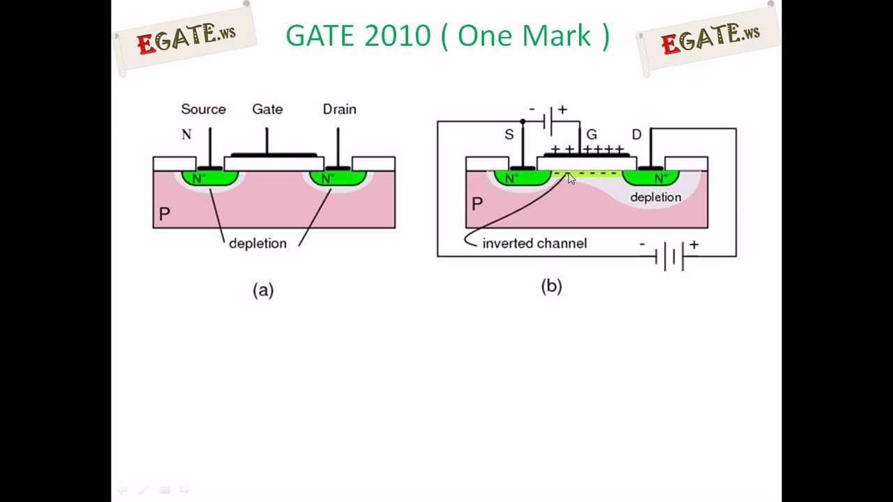
How do enhancement mode mosfets even work: You are missing the creation of the "Inversion" layer. When you apply positive gate bias to an enhancement mode mosfet, the existing P channel near the gate contact starts to recede and you have your gate contact - depletion region - p substrate. If you keep going, the concentration of holes near the contact is so little, that you form, in affect a N region near the contact - A N channel now forms between the source and drain contacts.

So at this point, is you examine a cross section of the Enhancement mode mosfet, from source to drain you will see: N+ - N - N+. If you now look "down" you will see Gate - N - depletion - P.

enter image description here

\$\endgroup\$
3
  • \$\begingroup\$ My question was based on a depletion type MOSFET which confuses me. Even more confusing is that the depletion type MOSFET works in an 'Enhancement mode' on changing the bias. If I apply the same logic, reverse bias should further shrink the n-channel rather than make it wider. That's what I don't understand. \$\endgroup\$
    – Sumanth
    Commented Nov 24, 2016 at 15:27
  • 1
    \$\begingroup\$ You should edit and make it a bit more clear what exactly you are asking.Enhancement mode and depletion mode mosfets behave the same way. The only difference is the presence or absence of a conducting channel "out of the box". Applying a positive bias to a depletion mode mosfet causes an even stronger inversion so the existing N channel becomes more N type thus more IDSS. The same applys to Enhancement types, you much first apply enough positive bias to create a channel, after that they will behave the same as the depletion types. \$\endgroup\$
    – MAM
    Commented Nov 24, 2016 at 16:06
  • \$\begingroup\$ So Depletion Mode mosfets can simply be thought as enhancement mode mosfets that have been turned on for you to begin with. \$\endgroup\$
    – MAM
    Commented Nov 24, 2016 at 16:07
3
\$\begingroup\$

People get into trouble when they ignore the movement of charge that is forming the channel. That charge has to come from somewhere. Typically there is a BULK tie/contact to inject this charge; the BULK may also be part of the reverse protection diode.

I've seen place-and-route projects that had to return to square-one and greatly increase the onchip BULK ties, because the sea-of-logic transients demanded so much charge from the (sparse) BULK ties that the propagation delays were horrid, and the jitter was horrid.

That 4rth terminal of the FET needs respect.

\$\endgroup\$

Your Answer

By clicking “Post Your Answer”, you agree to our terms of service and acknowledge you have read our privacy policy.

Not the answer you're looking for? Browse other questions tagged or ask your own question.