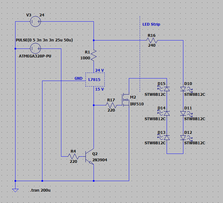
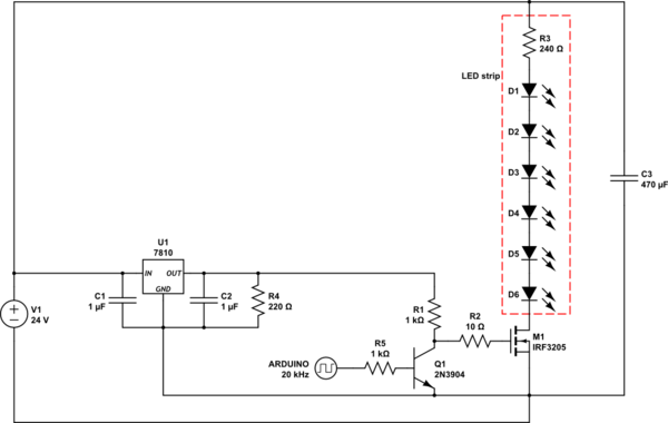
The overall design idea is on the right track, with the BJT acting as a gate driver for the MOSFET to bring its \$V_{GS}\$ up high enough for 5A of \$I_{ds}\$, and you seem to be grasping the basics, but there are some oversights that mean this isn't going to work.
(Un?)luckily for you, I've been working on a video series explaining exactly this topic, so I'm going to try to go through a whole design analysis here and explain all the gory details. This is a long answer, so maybe grab a beverage before you dive in :)
The first quick and easy fix is that R1 is in the wrong place. You want it after the regulator, not before.
You should also place a pair of 100nF ceramic decoupling capacitors physically close to the regulator - one between its output pin and ground pin, and the other between its input pin and a ground pin. Normally you'd want a fair bit more bulk decoupling than that, but your load current is small so you don't really need more.
The meat of the issue is that your MOSFET choice and R1 value look problematic.
The main concern is the on-resistance (\$R_{DS(on)}\$) rating for the IRF510, which is 0.54Ω at a gate-source voltage (\$V_{GS}\$) of 10V. No rating is given for a \$V_{GS}\$ of 15V, so we'll just use 10V here.
The dissipated power in the MOSFET will be \$P=I^2R\$, which is \$5^2 \times 0.54 = 13.5W\$. Given the junction-to-ambient thermal resistance (\$R_{thJA}\$) of 62°C/W, that's a temperature rise of \$13.5 \times 62 = 837°C\$. Your MOSFET is going to catch fire.
As a rough rule of thumb, you generally want to look for MOSFETs with an \$I_{DS(max)}\$ rating of at least twice your load current. You can then use its \$R_{DS(on)}\$ rating at the gate voltage you'll be using to figure out what the power dissipation will be, and then calculate the temperature rise using the thermal resistance rating of the package.
The 1kΩ value for R1 also seems like a problem due to the dynamic parameters of the MOSFET and your PWM frequency.
When Q2 switches off, current will start flowing from the regulator into the parasitic gate capacitance of M2. This current has to flow through R1 and R17. The total resistance ends up being 1220Ω plus the parasitic gate resistance (\$R_g\$) of the IRF510, which is a maximum of 11.6Ω. That means you've got 1231.6Ω of resistance in the gate charge path.
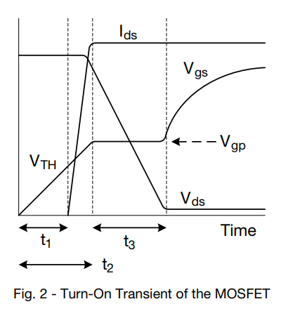
This appnote on MOSFET gate charge is useful for determining the time it will take to switch a MOSFET on with a given gate resistance. It splits the turn-on transient into three timing regions:

\$t_1\$ is the time it takes for the MOSFET to reach the threshold voltage, where it begins to conduct (i.e. \$I_{DS}\$ rises above zero). \$t_2\$ is the time it takes for the MOSFET to reach the Miller plateau, which is also where \$I_{DS}\$ reaches its peak. \$t_3\$ is the time it takes for the MOSFET to exit the Miller plateau once it has entered it.
Since your load current is 5A and the \$I_{DS(max)}\$ of the MOSFET is 5.6A, we can assume that \$t_2\$ is roughly equal to the amount of time it'll take for your load to be fully switched on.
We can use equation 12 from the appnote to calculate \$t_2\$:
$$t_2 = R_G \times C_{iss}\times ln \left( \frac 1 {1 - \frac {V_{gp}} {V_{GS}} } \right)$$
where \$t\$ is time, \$R_G\$ is the total resistance between the gate and the voltage source, \$C_{iss}\$ is the input capacitance of the capacitor, \$V_{gp}\$ is the gate plateau voltage, \$V_{GS}\$ is the gate voltage being driven, and \$ln\$ is the natural log function.
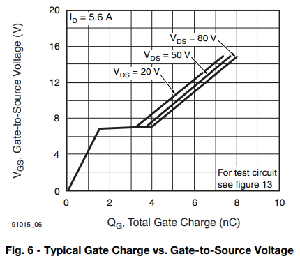
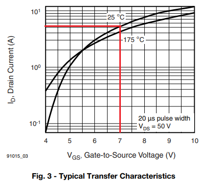
We can get the values for \$C_{iss}\$ and \$V_{gp}\$ from the IRF510 datasheet. \$C_{iss}\$ is listed on the dynamic parameters table, with a typical value of 180pF. The plateau voltage can be read from Fig 6 (Typical Gate charge vs. Gate-to-Source Voltage).

The gate plateau voltage is the \$V_{GS}\$ where the gate voltage "stalls" while the gate charge continues to increase, in this case around 7V. If you look at the \$V_{GS}\$ vs. \$I_D\$ graph (figure 3) from the datasheet, you can see that this aligns with the max rated current of 5.6A:

Based on these numbers, we can figure out the switch-on time:
$$t_2 = 1231.6\Omega \times 180pF \times ln \left( \frac 1 {1 - \frac {7V} {15V} } \right) = 139.4ns$$
You want to drive the gate with 20kHz PWM, which has a cycle period of 50 microseconds. This makes 139.4ns sound fast enough, but you actually need to consider the behaviour at the extremes of the duty cycle range. If you're using 8-bit PWM, the shortest pulse time is 1/255 of the cycle period, i.e. 196ns. This means that on the lowest duty cycle you're actually spending more than 70% of your time just switching the MOSFET on. This has implications for both power dissipation in your MOSFET (even if it wasn't already guaranteed to catch fire) due to the time the MOSFET spends in a resistive state, and for the minimum dimming level you can achieve.
The turn-off situation is the same in reverse but, since R1 is not involved in the turned-off state, the gate discharge path resistance is around 230Ω, which is a little less than one fifth the resistance of the gate charge path. Since \$t_2\$ is proportional to \$R_G\$, we can estimate that it takes around 30ns to turn the MOSFET back off (based on a rough estimate of \$t_3\$). So at high duty cycles (e.g. 254/255) you'll still be ok.
All of this is to say that you're going to have trouble with this design and component choice.
Now, how do you fix this?
First, you're going to need a better MOSFET. Pick one with an \$I_{DS(max)}\$ of at least 10A. I'd personally look for something around 15-20A, since the price difference is going to be essentially zero. Make sure its \$V_{GS(max)}\$ exceeds 15V (unless you choose to use a logic-level MOSFET; more on that later). Then figure out what the \$R_{DS(on)}\$ will be at 15V, and use \$P=I^2R\$ to calculate the power dissipation in the MOSFET in its on-state. Multiply that by the \$R_{thJA}\$ of the package to figure out the worst case temperature rise above ambient. Ideally you want to keep this small, because all the other parameters of the MOSFET will start to derate as the temperature climbs. Remember that you need to add your worst-case ambient temperature to the temperature rise to get the actual operating temperature.
Next, you need to reconsider your driver circuit. It's ok for slow switching, but for 20kHz 8-bit PWM it's not great.
The first thing to consider is R17. MOSFET gate resistors aren't used for the same reason as base resistors on BJTs. With a BJT you need a gate resistor to limit the \$I_{BE}\$ current. With a MOSFET, gate resistors can often be omitted entirely.
A common case where you might want to include a gate resistor is if you're driving the gate directly from a GPIO pin, since you want to limit the current flowing in/out of that pin to within the max source/sink current rating of the GPIO. In such a case you can use Ohm's law to figure out the resistance you need - you've got a GPIO pin at a given VCC voltage, connected to a discharged gate at 0V, and the MCU's datasheet will tell you the maximum current you can draw/sink. So you can use \$R=\frac V I\$ to calculate the necessary gate resistance.
Gate resistors are also sometimes used to prevent ringing and EMI on gate drivers when switching MOSFETs very quickly (hundreds of kHz or MHz).
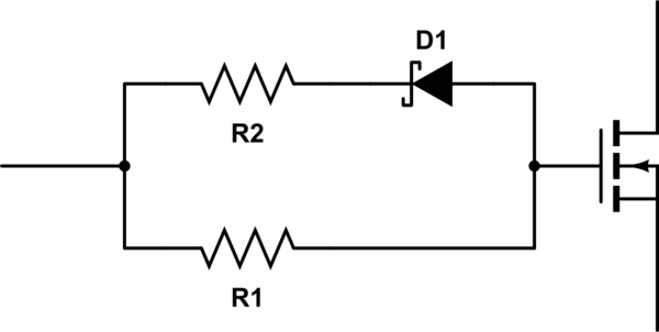
You'll also sometimes see a configuration where two resistors are placed in parallel, with one resistor having a diode in series with it:

simulate this circuit – Schematic created using CircuitLab
This is used for asymmetric gate drive current. R2 is lower than R1. When the gate is being charged, the current must pass through R1. When the gate is being discharged, the current can pass through R1 and D1/R2, so the gate can discharge more quickly. This avoids a problem called parasitic self-turn-on, which is to do with the plateau we saw above in the gate charge graph. Essentially, while the MOSFET is in the process of turning off, the parasitic capacitance at the MOSFET gate can create a capacitive voltage divider effect between the drain, gate, and source, and cause the internal voltage at the gate to jump back up, above \$V_{gs(th)}\$, which causes the MOSFET to unexpectedly turn itself back on! This can be catastrophic in push-pull configurations because it leads to shoot-through, where the supply rail is essentially shorted to ground through the MOSFETs. This isn't so much of a worry for your use-case.
If you remove R17, that takes care of part of the problem, but you've still got a bunch of resistance from R1. The problem now is that if you reduce R1 to get lower gate charge resistance, you're shunting much more current through Q2 while it is switched on, which is inefficient and is going to heat up both R1 and Q2. Finding a balance between a low enough R1 to get good switching performance but high enough R1 to avoid wasting power and heating up your components is tricky.
Luckily there are other options.
The easiest is to just buy a logic-level MOSFET that'll handle 5A of \$I_{DS}\$ with a \$V_{GS}\$ of 5V or less, and drive the gate from the GPIO with a 120Ω resistor in series with the gate (based on 40mA max GPIO current and 5V drive).
If you can't find a logic-level MOSFET that'll fit your requirements (or it's too expensive) you can use a MOSFET driver IC. For your case you want a low-side MOSFET driver. They're cheap and super simple - typically you'll have a power pin, ground pin, gate drive pin, and logic level input pin. You give it some power, hook the input pin to a GPIO, the gate drive pin to the gate (possibly through a small series resistor - see the driver datasheet for details), and that's it. It does all the driving magic for you!
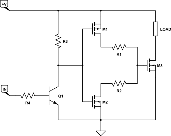
Alternatively, if you're set on building your own MOSFET driver from discrete parts, you can construct a push-pull driver. There are lots of designs for this, but I'm a fan of an adaptation of Prof. Sam Ben-Yaakov's split resistor push-pull driver from this video.

simulate this circuit
The linked video explains it in detail, but here's a quick overview:
- M1 and M2 are small MOSFETs (P-channel on top, N-channel on bottom) which form a push-pull driver. These are chosen with a \$V_{GS(max)}\$ high enough to withstand the gate drive voltage.
- R1 and R2 are asymmetric drive resistors. R1 is typically larger than R2. This allows M3's gate to discharge more quickly than it charges, and avoid any self turn on effects. Sensible values for most cases are somewhere around 10Ω for R1 and 2Ω for R2. Typically R1 and R2 are both rated for 1W or so (rather than 1/16W or 1/8W of your typical SMD resistor) so that they can handle the short high-current pulses during switching transients.
- Q1 acts as a voltage level translator from the output voltage of the MCU to the MOSFET gate drive voltage.
- When the input is high, Q1 switches on, and pulls the gates of M1 and M2 to 0V.
- Since M1 is a P-channel FET, a low gate-source voltage means it switches on, so a current flows through it and charges M3's gate through R1.
- Since M2 is an N-channel FET, a low gate-source voltage means it switches off, so it does not conduct and no current can flow through R2 and M2 to ground.
- When the input is low, Q1 switches off, and R3 pulls the gates of M1 and M2 high. Since M1 and M2 are small, and they aren't switching large currents, they have low effective gate capacitance and can be quickly switched without a lot of current, so it's ok if R3 is 1kΩ or more.
- Since M1 is a P-channel FET, a high gate-source voltage means it switches off, and no current can flow through it.
- Since M2 is an N-channel FET, a high gate-source voltage means it switches on, and M3's gate discharges through R2.
- If M1 and M2 don't turn on/off at the exact same rate, both of them could be conducting at once. This is the main problem with push-pull drivers, because you get shoot-through where there's a path from power to ground through the MOSFETs. However, in this configuration, the path has to go through M1, through R1, through R2, through M2, and then to ground. This increases the total resistance of the shoot-through path. If you test this out, it turns out that the magnitude of the transient shoot-through energy is lower than the magnitude of the gate drive energy. This is much better than other designs.
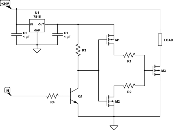
If you want the gate drive voltage to be different to the load drive voltage, you can take the same approach as in your original circuit:

simulate this circuit
If you're scratching your head a bit, don't worry. High speed MOSFET drivers are actually hard work to build. Understanding them is a lot of fun, but if you just want to get on with a design then you can skip the design lesson and just opt for a logic-level MOSFET or a gate driver IC.
And that's just about it. I hope you learned a bunch :)
As a very last quick aside, something to watch out for is the base current when you're driving BJTs from a GPIO. A 220Ω base resistor (R4) is probably a little on the low side. With your MCU outputting 5V, you'll have about 20mA of current flowing from the Arduino's GPIO into the base of Q2. That's within the limits of the Atmega328P, but it's still a bit excessive, and with other MCUs you might not be allowed to source as much as 20mA from a GPIO pin. The current amplification behaviour of a BJT is roughly \$I_C = I_B \times \beta\$ (where \$\beta\$ is sometimes listed as \$h_{FE}\$ in datasheets). Given that \$\beta\$ is in the range of 100-300 for the 2N3904 in the design you're using, 20mA of gate current gets you anywhere between 2A and 6A of \$I_{CE}\$ current, which is more than enough. You can tone down the base current a bit. Alternatively, you can just swap the BJT out for a small N-channel MOSFET (e.g. 2N7002) in exactly the same configuration and not worry about base current at all.

