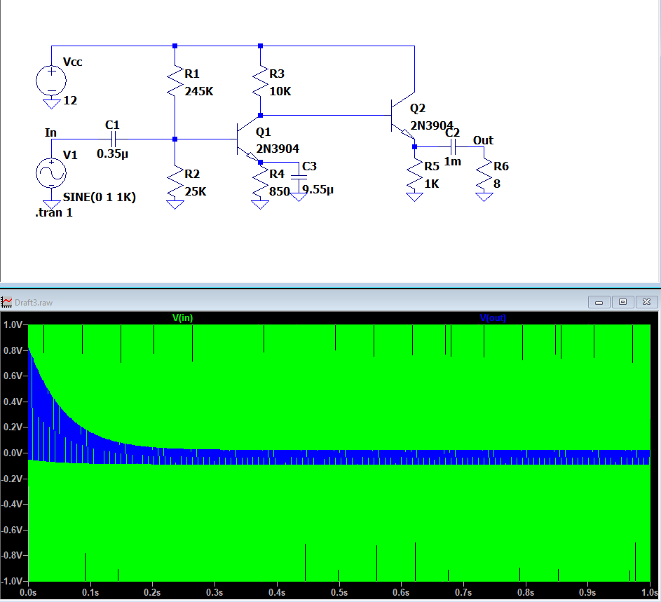
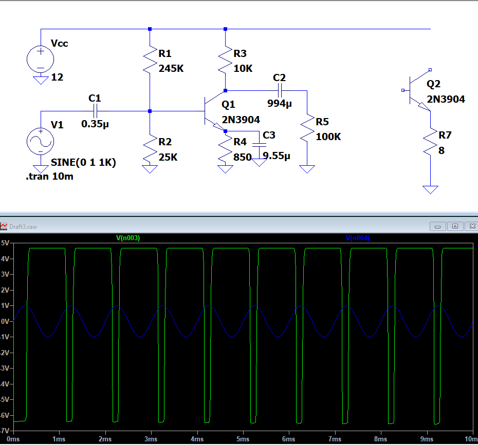
2
\$\begingroup\$

enter image description here

enter image description here

Goal of the circuit:

  • Must be able to deliver 1.5 W to the speaker (8 Ω) at 1 kHz.

First Problem

1.) how can we drive an 8 ohm speaker if it can only support around 1.5-2 watts? Because when we input 8ohms as the load the Vout decreases.

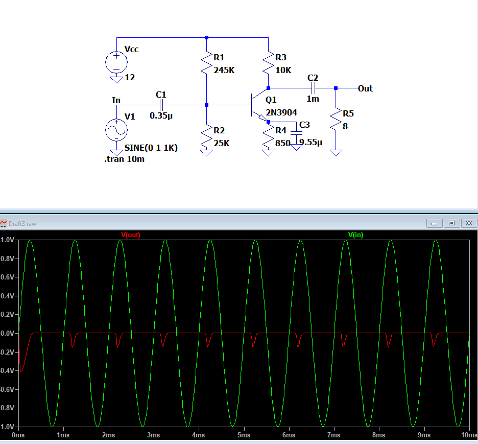
  • Coupling capacitor formula we used is 1/2pi(lowest frequency)(resistance seen by capacitance) 20Hz was the lowest frequency I used.

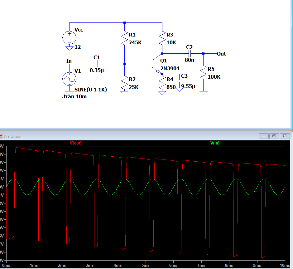
Referencing to the image above. If we add a common emitter by our understanding it should increase the power but even with coupling capacitor, it won't shift down to AC.

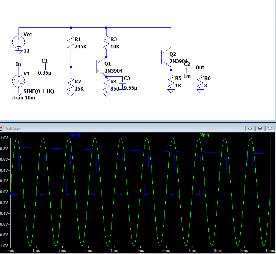
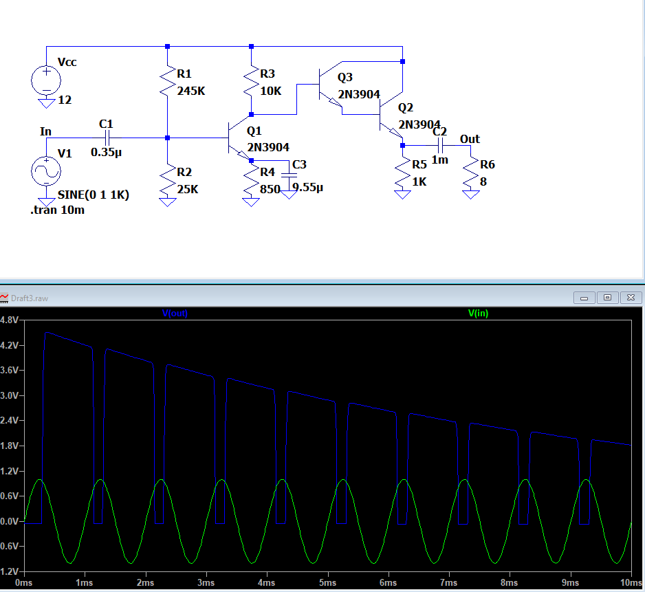
The next step we did was thinking of adding a darlington pair, it did increase the gain, but it still doesn't want to make the AC waveform shift down to its negative half cycles for a safer speaker usage.

enter image description here

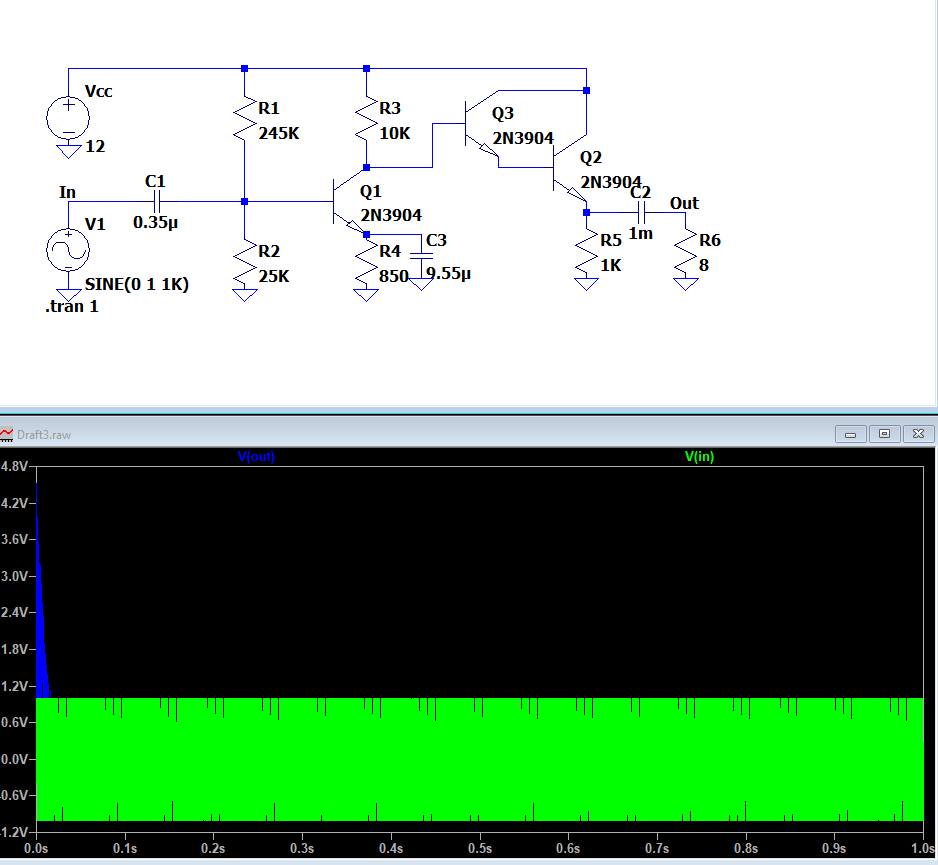
above is the darlington w/ ce and ef (1s)

enter image description here

above is without the darlington.

Summary

Our goal is to get the output that is the same in the photo below. note The RL (R6) is 100K ohms but we want that output if our desired Load is an 8ohms 2W Speaker, that can ultimately support 1.5-2W power for the speaker. What changes can we implement in our design to achieve this?

enter image description here

\$\endgroup\$
7
  • 3
    \$\begingroup\$ All of these schematics and waveforms are useless unless you show us the reasoning and the equations you're using to come up with these component values. We also need to see the rest of the requirements -- specifically, what are the characteristics of the signal source? Only then can we talk about where you're going wrong. \$\endgroup\$
    – Dave Tweed
    Commented Jan 18 at 13:02
  • 2
    \$\begingroup\$ Get an audio amp IC. If it's forbidden try a discrete push-pull.amp. If it's forbidden, too, you must improve your current attempt substantially. You very likely have seen this case electronics.stackexchange.com/questions/697554/… Maybe today is a good day to read it. A single ended linearly amplifying output stage will unavoidably dissipate at least 2W for 2W audio AC output, probably more, because you want to avoid inductive parts, I guess. \$\endgroup\$
    – unawriter
    Commented Jan 18 at 13:45
  • \$\begingroup\$ Seems you're focus is on a Class-A design. If you proceed this way, you're move to Darlington is in the right direction. However you'll need a bigger transistor in the Darlington-pair than 2N3904, with DC bias far greater so that AC power output is larger. \$\endgroup\$
    – glen_geek
    Commented Jan 18 at 14:24
  • 3
    \$\begingroup\$ Jax, I think I keep seeing you post over and over on this same topology. It's not going to work. You need to break yourself of this. So stop thinking there's a way to fix it. There isn't. It's the wrong tool for the job. Full stop. \$\endgroup\$ Commented Jan 18 at 20:09
  • 1
    \$\begingroup\$ Jax, You're making your own darlington from two transistors? The first one can be a 2N3904, because it only passes fairly low current. But the second transistor must pass a great deal more current, and should be a power transistor, likely on a heat sink. It's emitter resistor should be small, below 10 ohms so that about 0.8 A flows. You should look for a transistor whose \$IC_{max}\$ is above 2A. \$\endgroup\$
    – glen_geek
    Commented Jan 19 at 14:48

3 Answers 3

1
\$\begingroup\$

Its okay not to know what to do right away. But my advice is your darlington approach is okay however if you check LT spice your power is incredibly low from what your target 2W. I may resuggest unawriter advice to directly put push and pull amplifier. I would recommend a class AB see here for more info about this.

I would suggest to put it directly on your output. And try to play around with your values use your knowledge about capacitor coupling and biasing for this.

May I also suggest to check this post I have recently read it and it quite match your question.

\$\endgroup\$
4
\$\begingroup\$

I sincerely wish you'd give up on the 2nd stage -- the power output stage -- that you keep insisting on using. It's useful if and only if you want lots of heat and/or fire and/or a rapid unplanned/unscheduled disassembly.

The 2nd stage is not salvageable. So I'm not wasting more time on it. You can read something I wrote, recently, here.

It's just wrong. Abandon it.

On the first stage, the main problem is that it is highly distorting, due to a widely variable voltage gain that depends upon the applied signal, itself.

Let's first look at the DC bias operating point (quiescent operation):
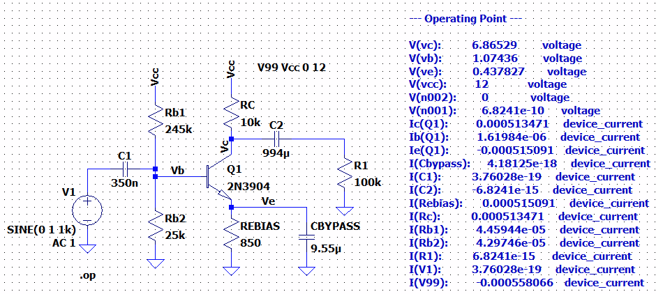
enter image description here

From that, and the emitter bypass capacitor arrangement, I can estimate the small signal voltage gain as about \$45\:\text{dB}\$ (for the case where the applied input signal is extremely tiny -- negligibly so.)

(I'm going to ignore the base biasing pair as they look stiff enough to me, upon first glance.)

Based upon two facts observed from the DC quiescent bias point of \$V_{_\text{C}}\approx 6.9\:\text{V}\$ and \$V_{_\text{E}}\approx 440\:\text{mV}\$, and keeping in mind that the minimum \$V_{_\text{CE}}\approx 1\:\text{V}\$, I'd estimate that the maximum input signal magnitude can be no more than \$30\:\text{mV}\$ peak. Yet you are applying a test value of \$1000\:\text{mV}\$ peak! Right off the bat, that's not going to work.

Let's test my assertion:
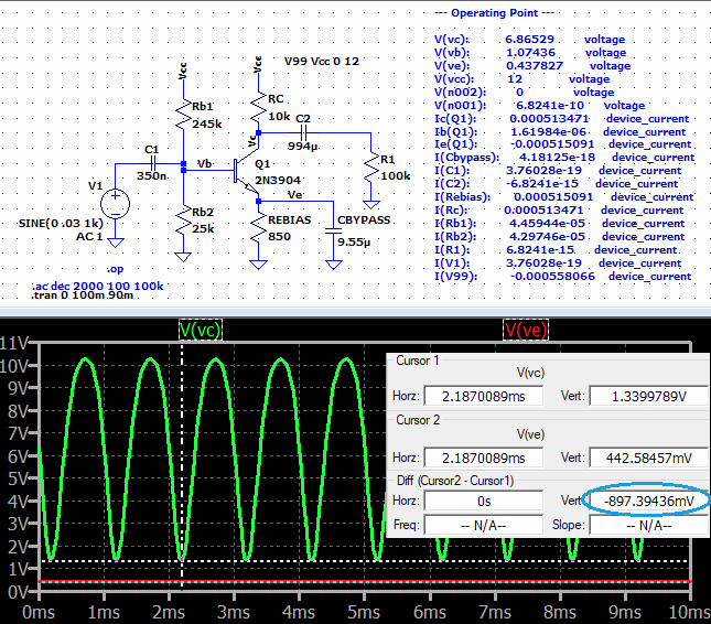
enter image description here

First off, yes. With an input of \$30\:\text{mV}\$ peak, we just break through my \$V_{_\text{CE}}\approx 1\:\text{V}\$ (to avoid the onset of saturation.) Close enough so that my approach is validated.

But second, notice the terrible distortion in the green curves? That's what this kind of stage does to an input signal when pushing it to its limits. This is because the voltage gain is highly variable with input signal, if the input signal deviates very far from its small signal assumption. And a \$30\:\text{mV}\$ peak obviously falsifies that assumption.

Earlier, I said the voltage gain is \$45\:\text{dB}\$. This would be truer for a \$1\:\mu\text{V}\$ input peak. But with the collector dropping to \$1.4\:\text{V}\$, the change in collector current is substantial (more than double) and this changes the voltage gain by the same factor, to almost \$53\:\text{dB}\$. Similarly, at the other end of the cycle the collector current drops by about a factor of 4 now and therefore the voltage gain drops to about \$33\:\text{dB}\$.

Those kinds of voltage gain changes mean distortion on an epic scale!

You just can't do that.

There are fixes. One fix is to dramatically reduce the input signal (I'll get to that, shortly.) Another would be to add global NFB (with another transistor added.) And another would be to place an AC emitter degeneration resistor in series with the emitter bypass capacitor. That will reduce the gain. But that's the price that has to be paid to keep this topology.

What signal level would be acceptable? That depends on how much distortion you are willing to accept. But let's say a gain variation of \$\pm 3\:\text{dB}\$ is acceptable (a factor of \$\sqrt{2}\$ in collector current, one way or the other.) Then the maximum input signal would be about \$9\:\text{mV}\$ peak!

Let's see:
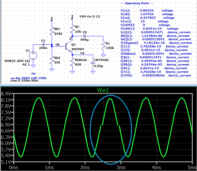
enter image description here

And that looks a lot better. But as you can see, where I flipped one half-cycle around in the center, it's still distorting the input signal enough to notice here.

So you have the above issues with respect to the 1st stage, which need solutions. And the 2nd stage is simply wrong and needs to be abandoned, entirely.

\$\endgroup\$
1
\$\begingroup\$

There are several problems with the base design, not the least of which is that a 2N3904 cannot supply the current needed without burning up (IRL).

In each of the schematic with an output emitter follower (not an output common emitter), the emitter resistor R5 is 1K. During positive half-cycles of the signal, the output current is supplied by the Q2 or Q2-Q3. During negative half-cycles, the current path is though R5 only. Thus there is a 1K resistor in series with the 8 ohm load.

If you reduce R5 to 1 ohm, 8 ohm load will have a much more symmetrical current path for the entire cycle. The circuit probably will simulate much better, although it will not work in real life.

Please add figure numbers to each image so we can be sure which schematic is being discussed.

\$\endgroup\$
1
  • \$\begingroup\$ do you think maybe it being not centered is such a big deal? or maybe it will just be a nuisance when prototyping so it would help if any problem comes up we can rule this out. We haven't prototyped yet so insights on how this can go would really help. \$\endgroup\$ Commented Jan 19 at 6:58

Your Answer

By clicking “Post Your Answer”, you agree to our terms of service and acknowledge you have read our privacy policy.

Not the answer you're looking for? Browse other questions tagged or ask your own question.