I was browsing Google images of LTZ1000 voltage reference IC. I saw that in some of the PCBs, the traces that go to LTZ1000 are in spiral shape and cut out gaps are left between them. What is the reason behind this?
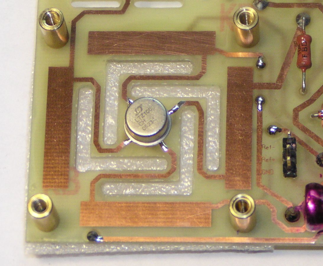
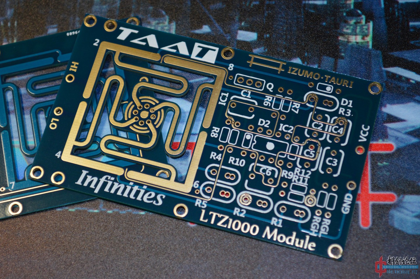
I was browsing Google images of LTZ1000 voltage reference IC. I saw that in some of the PCBs, the traces that go to LTZ1000 are in spiral shape and cut out gaps are left between them. What is the reason behind this?


It is to reduce the thermal gradient across the device.
A longer meandered track will carry less heat to and through the part than a short straight track. Note also that the PCB substrate has been milled away between the tracks; the PCB probably conducts most of the heat.
We normally think of a PCB as performing mainly the electrical function of connecting the parts together, and the mechanical function of holding them securely. As the manufacturing process is simple, reliable and accurate, PCBs are also useful for simple mechanical engineering tasks like this.
The datasheet says:
Thermocouple effects are one of the worst problems and can give apparent drifts of many ppm/°C as well as cause low frequency noise. The kovar input leads of the TO-5 package form thermocouples when connected to copper PC boards. These thermocouples generate outputs of 35µV/°C. It is mandatory to keep the zener and transistor leads at the same temperature, otherwise 1ppm to 5ppm shifts in the output voltage can easily be expected from these thermocouples.
So the elaborate board design seems specifically to counter this thermocouple effect. The thin leads and cutouts increase the thermal resistance from rest-of-board to the device, and the circular patterns near and under it try to keep the footprint a highly conductive region.
As well as the reasons given (thermal EMFs, mainly, mechanical stresses I think are less of an issue with TO5 than with a SMT reference) it will also reduce power consumption. The LTZ1000 is normally run in an (internally) ovenized mode with the die at perhaps 70C so it is a major heat source on the board with relatively vast (for a precision circuit) quantities of heat flowing radially outward from the device to the surrounding PCB. By reducing thermal losses through the board (and keeping the board at the leads solid and with something like a ground plane), disturbances and losses can be minimized.
By increasing thermal resistance in relation to the thermal mass at the package, the temperature controller will be able to maintain the temperature of the die (and thus the buried zener reference junction) more constant, all other things being equal.
Finally in a typical LTZ1000 application there will be other parts which could be affected by thermal gradients on the PCB caused by having a part with large and varying power dissipation. The thermal isolation helps with that too.
Of course, ovenizing the entire circuit might be better from a stability point of view (not leakage though, unless the 'oven' can cool too), but that's often impractical. An array of LTZ1000 devices can be used to get somewhat better stability (ideally improving with he square root of the quantity of devices)- expensive but not in the range of Coulomb blockade devices.
In addition to minimizing direct thermal effects, the PCB is milled away in order to minimize the mechanical stress that is put on the leads by the expansion and contraction of the rest of the PCB. Such stresses can be transmitted to the package and directly to the silicon inside, causing undesired voltage offsets.
Dave Jones discusses this in a recent EEVblog video.