2
\$\begingroup\$

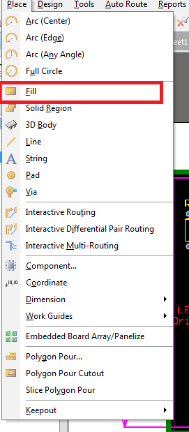
Recently I saw a PCB which was all Ground and other Nets were Routed inside that. I found out that in order to do that (In DXP software) you have to do as following:

enter image description here

But the question is what is the reason of doing that?

Is that recommended to do it for all kind of circuits at all? Is that possible to make it all VCC? what would be the differences?

\$\endgroup\$
1
  • 1
    \$\begingroup\$ "Fill" will make a rectangular shape. "Polygon Pour" is much more useful. It will make an arbitrary shape that automatically flows around other features so you don't have to keep adjusting it to make room for components/tracks/etc. \$\endgroup\$
    – The Photon
    Commented Aug 31, 2013 at 15:28

2 Answers 2

5
\$\begingroup\$

You usually do that in multilayer designs where you designate specific layers to certain power nets such as 3V3 or GND. the intended goal is to make the supply and return path of the current as short as possible (also, the two layers form some kind of small capacitance). If it's on the outside layers, it's sometimes done to block RF from leaving the inner layers. Also, it's nice for production since it reduces the amount of copper which needs to be etched away.

Well, most of all: it's a combination :-)

In Altium you might not want to use fills but instead you will be using polygons where you can specify the connect style (if you want the connection to be a thermal relief). Also, using the Layer Stack Manager you can specify specific layers to be power planes which basically makes them "inverted". So as long as you do not draw a line on such a layer, the full layer will be connected to a specific net. By drawing lines (thereby separating two areas) you can create so called split-power planes.
\$\endgroup\$
8
  • \$\begingroup\$ What if I want to have a single layer design? does it have any benefit in this scenario? can I route some other net from inside the filled Net (in single layer design)? \$\endgroup\$ Commented Aug 31, 2013 at 11:47
  • \$\begingroup\$ Sure, simply consider a fill a large track (often, the fill is connected to GND in such a design). Though I never haven't seen any advantage to using a polygon. As for the polygon, you can draw it over other tracks and it will automatically break where other tracks are (plus you can easily shelve and then restore polygons in Altium). Also see: wiki.altium.com/display/ADOH/Polygon+Pour \$\endgroup\$
    – Tom L.
    Commented Aug 31, 2013 at 12:35
  • \$\begingroup\$ One more thing. If you use a polygon, you can simply draw a polygon over the whole board area and this will make what you saw (where there are no tracks or other fills/polygons there will be a ground polygon). \$\endgroup\$
    – Tom L.
    Commented Aug 31, 2013 at 13:30
  • \$\begingroup\$ You know I am doing this but I faced with a problem. After I use polygon or fill, how can I do the routing? shall I at first pour the polygon or shall I at first route the connections and then pour the polygon? \$\endgroup\$ Commented Aug 31, 2013 at 14:10
  • 2
    \$\begingroup\$ You can do the following: At the beginning you can pour a polygon over the whole area. Then use the "Shelve Polygon" command to "shelve" it. This means that you can now route just like there was no polygon. When you're done (or sometime in between), use the Re-Pour Polygon command to repour the polygon (Altium will know where it was and will pour copper except for your tracks). So the main topic is: Try out the pour and shelve polygon commands. \$\endgroup\$
    – Tom L.
    Commented Aug 31, 2013 at 18:52
2
\$\begingroup\$

Ground planes are pretty common in PCB design. They act as shielding from outer electromagnetic radiation, therefore reduce noise cached from the outside. Also tend to reduce crosstalk when ground trace is placed between signal traces. The drawback of such planes is that they introduce higher capacitance between signals and the ground, what is relevant for high frequency circuits. That is why hatched pours are also used as introduce smaller capacitance.

Regarding Supply planes they effectively act as wide traces, improving current handling and reducing voltage drop on such trace. If such plane provides supply to other layer, number and size of connecting vias has to be taken into account as can be bottleneck of current path.

\$\endgroup\$

Your Answer

By clicking “Post Your Answer”, you agree to our terms of service and acknowledge you have read our privacy policy.

Not the answer you're looking for? Browse other questions tagged or ask your own question.