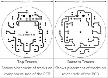
I'm trying a DIY PCB using toner transfer method then etching but I am confused with the diagram below. I thought the top trace goes to the copper board but there's this bottom trace which shows solder side. Which of the two goes to the copper side? Any help would be greatly appreciated thanks.
-
3\$\begingroup\$ Is this 2-layer PCB? In that case both sides should be "copper side". \$\endgroup\$– Eugene Sh.Commented Sep 19, 2017 at 15:38
-
1\$\begingroup\$ It's a dual sided PCB, you want a board with copper on both sides \$\endgroup\$– ratchet freakCommented Sep 19, 2017 at 15:38
-
1\$\begingroup\$ But I am not quite sure how you are going to align the layers on both sides with this technique. I would think of drilling few reference holes... \$\endgroup\$– Eugene Sh.Commented Sep 19, 2017 at 15:40
-
\$\begingroup\$ Can't imagine why you would consider making one when they are so cheap....pcboard.ca/kits-and-boards/blank-project-pcbs/… Also track and pad sizes are probably a bit fine for home builds and through hole plating/soldering will be an issue. \$\endgroup\$– Trevor_GCommented Sep 19, 2017 at 15:51
-
\$\begingroup\$ @EugeneSh. presumably you would cut it to a circle after etching is complete. That way to can have a reference edge/corner. \$\endgroup\$– ratchet freakCommented Sep 19, 2017 at 15:57
2 Answers
This is a design for a two-sided board. You need to have copper on both sides of the board and etch each one according to the provided pattern to make this circuit.
Edit: FWIW, I agree with the other answers and comments saying this board as drawn is not a great candidate for toner transfer. However it should not be difficult to re-design this as a one-sided design, probably with a few jumpers. Or simply pay a few dollars and wait a couple weeks to have it built for you.
-
\$\begingroup\$ Oh thank you, the website this diagram came from didn't have instructions or anything. I am new to PCB making so I didn't know. \$\endgroup\$ Commented Sep 19, 2017 at 15:43
To make transfers on bottom side, create the mirror image. These are TOP view of top and BOT.
Add 4 corner dots and verify scale coordinates after print. Then use for alignment with centre.
You are better off buying this, but ok. You have to learn the hard way.
This design has lots of holes with no vias which wont fill from bottom side soldering.
Get strong stubby drill bits, and use a mini drill stand.
Make a material spacer standoff for the LED's , otherwise risking goldwire shear solder stress failures inside or lack of room to reflow solder to top side without vias. Using sufficient heat allow only 3 sec. absolute max to apply heat and solder at the same time. .
BTW most of these top side tracks could be done on BOT layer and with a 1 sided board with a couple jumper wires. I would strongly suggest, you modify the artwork to 1 sided since you have too many vias to fill top and bottom side with LEDs being extremely ESD and solder senstive.
I once flew to NZ to fix a customer's field failures because of lack of awareness to the above.
-
\$\begingroup\$ +1. I agree wholeheartedly. I would not even think about attempting this one with kitchen gadgets. Esp not when I can buy it for less that it would cost me to make it. \$\endgroup\$– Trevor_GCommented Sep 19, 2017 at 16:16

