0
\$\begingroup\$

I'm currently trying to adapt a single li-ion battery charger based on the TP4056 to work with charging more than one battery. The idea is to use a logic circuit that is controlled by the IC's "FULL" output signal. Whenever the first battery is charged, the signal goes high and an LED switches on; the logic should then switch such that the charger is then connected to the second battery. Whenever that is charged, the charger should switch off (rather than switching back to the first, to avoid rapid switching). This has proved more difficult than I expected to design.

RM TP4056 datasheet here - presumably what you had in mind?

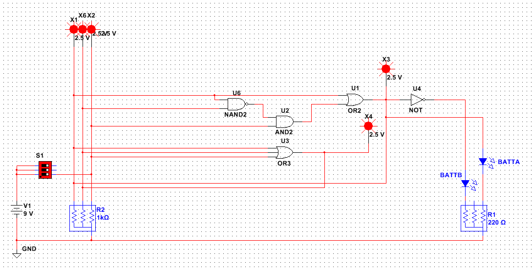
A friend of mine designed a circuit that should apparently do the trick, although it doesn't factor in propagation times and has one or two wrong connections which he later pointed out.


(source: pomf.se)

This is what he said about it:

ah I think I wired the outputs wrong. Like I said, I was being lazy. X3 stays off while something needs charged X4, which isn't connected switches between a and b. so those two wires and the inverter connected to the leds should go to x4 not x3

With these in mind, is this circuit likely to work (once appropriate delay is used in case propagation times compromise switching)? It seems to me that the 3-input OR is a overkill, and that the same thing would be achieved by removing the left-most rail (indicated by X1), replacing the 3-input OR with a 2-input, changing the NAND at the top to a NOT, and removing the connection between the X1 rail and the U1 OR gate. Please advise.

\$\endgroup\$
3
  • \$\begingroup\$ Your schematic doesn't show the TP4056 battery charger or power switching, only some logic controlling LEDs. What are the Xn points connected to? There's no way to know what is going on in the power portion of the circuit from this diagram. \$\endgroup\$
    – Matt B.
    Commented Aug 10, 2014 at 18:33
  • \$\begingroup\$ Most of the Xns were simply added as probes for testing voltages. X3 controls power to the charger, so it should go high whenever both batteries are charged. The input at S1 is the FULL sensor; it goes high whenever the TP4056 outputs a full signal, that is, whenever the current charging battery is full. \$\endgroup\$ Commented Aug 10, 2014 at 20:28
  • \$\begingroup\$ @AlexFreeman - See changes to my answer including comment on 1 IC solution. \$\endgroup\$
    – Russell McMahon
    Commented Aug 11, 2014 at 7:40

3 Answers 3

2
\$\begingroup\$

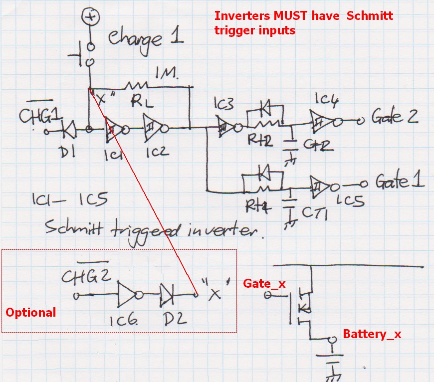
This (untested*) circuit should do exactly what you specify.
Adding the optional inverter and diode should cause it to toggle to and fro between batteries once the current one is charged.

Operation:

enter image description here

Push button starts charging at battery 1.
IC1 + IC2 + Rl form a latch.
Pushbutton High sets latch output to high.
Chg1 low sets latch output to low.
Rl provides feedback to IC1 + IC2 which form a non-inverting buffer.

Latch high sets IC5 in high after time delay due to Rt1, Ct1.
So IC5 out goes low after time delay and FET1 is turned on by low gate signal.
Gate 2 is high (trace it through).

When battery 1 is charged signal CHG1 goes low.
IC1 in low so IC2 out low so latch out low.
Even when CHG1 goes high again latch will stay in low state.
IC5 in is taken low by CT1 discharging via diode so minimal delay.
IC3 in low sets IC4 in high after delay due to Rt2, Ct2.
So IC4 out low after delay and FET 2 on and battery 2 charges.

When Battery 2 is charged either just let TP4056 stop charging (as it does) and signal end of charge with LED,
OR use optional circuit at lower left with IC6, D2 to set latch input high and swap back to first battery.

Depending on TP4056 behaviour this may or may not be a good idea. There may be a small charge period while the TP4056 determines that the battery is charged. The circuit should toggle to and from between the two batteries. How much charging occurs depends on several factors but it is undesirable to add substantial extra charge at this state.


Switch: A MOSFET switch is shown. Note that the charger voltage needs to be greater than battery voltage to present back feeding via the body diode. This is not a fault of the logic but a limitation of MOSFETs as switches. This 'feature' may be overcome by using either a relay or back to back MOSFETS. [Two P Channel FETS. Connect gate to gate and source to source. Two drains are input and output (either polarity). Drive connected gates with gate drive. (Despite what may be intuitive this arrangement DOES start when driven. The nervous may add a say 1 megohm resistor from the connected sources to V+. MOSFET Vgs_max must be less than supply voltage. FET Vth needs to be suitable for drive voltage used - say 2V or less in this application.


  • Untested: This circuit has neither been built nor simulated. However, I have built about 5 zillion** circuits over too many decades using a 74C14 or similar in analog mode as used here. It's entirely possible that I've missed something or done something stupid but odds are it will work OK. If not, remove the purposeful error (cough) placed there as part of the student's training (cough) and proceed.

** On average 1 zillion per decade.

\$\endgroup\$
7
  • \$\begingroup\$ Right, very nice. This looks very much feasible. A few things though: -Can I use a comparator with feedback to make the schmitt inverters? -Why do the inverters need hysteresis? -Can IC1 and IC2 be replaced with anything? A dual inverter seems a little redundant to me. \$\endgroup\$ Commented Aug 11, 2014 at 21:43
  • \$\begingroup\$ @AlexFreeman You can use comparators BUT the gates use less components, probably cost less and, once you see what can be done with them, provide you with decades of new solutions :-). | IC1+2 form a latch because they have zero inversion end to end and Rl provides positive feedback. Any input that can overcome Rl feedback controls the latch - here /CHG or pushbutton. A cheaper simpler latch is hard to come by. | Hysteresis turns the gradual analog transitions into sharp digital edges. IC4 and IC5 provide sharp on/off gate drive signals derived from the RC delays. The Rtx diodes .... \$\endgroup\$
    – Russell McMahon
    Commented Aug 11, 2014 at 21:49
  • \$\begingroup\$ @AlexFreeman .... make the delays asymmetric - Caps charge positively slowly and discharge rapidly. This gives the non overlap function as when one gate turns off it does so soon after transition while the matching turn on is delayed. The hysteresis stops these signals being a soggy mess. | The Schmitt gates can also act as an oscillator (1 gate), PWM converter or audio amplifier (!!!) 1 gate, much more .... . \$\endgroup\$
    – Russell McMahon
    Commented Aug 11, 2014 at 21:53
  • \$\begingroup\$ Right, but, I'd rather work with the components I have, rather than buying new ones if i can avoid it. I currently have a bunch of comparators, amplifiers, NAND gates, and of course all necessary passive components. I'm trying to build this as soon as possible so i'd rather not order in anything if i can build it with what I have here. \$\endgroup\$ Commented Aug 11, 2014 at 22:52
  • \$\begingroup\$ @AlexFreeman - Understood BUT the only part you do not have is the hex Schmitt inverters, they cost very little, they come in little time, they use far less parts for this and other tasks AND once you realise what you can do with them they are your friend for life. | bout 30c to 40c each in 10's at Digikey. \$\endgroup\$
    – Russell McMahon
    Commented Aug 12, 2014 at 13:14
1
\$\begingroup\$

Important points:

(1) The charger will stop charging when the battery is fully charged". Overcharging will never occur due to the charger IC being permanently applied.

(2) If you apply the charger to a fully charged cell the worst that is liable to happen is that V_max_charge (typically 4.2V) will be applied for a brief period, the battery will start to accept a small amount of current < I_charged_minimum and charging will then stop again. How long this small charging "blip" lasts for is up to the IC designer but it will probably be a small fraction of a second. This will have the effect of very slowly adding to the battery charge even when it is deemed fully charged, but the rate will be very low. eg if you cycle every 60 seconds so that a charging "blip" occurs every 60 seconds and if the blip lasts 1 second (probably far less) and if I_charging_min is 25% then the effective charge rate is Imax x 1s/60s x 25% or C/240 for a typical cell rated at max charge rate of C. It will probably be less to much less than this in practice.

(3) I note below the use of relay or MOSFET as a switch. If a MOSFET is used in eg a simple high side switch arrangement then there is the potential for each to back discharge into the charger circuit when the MOSFET is off if Vbat is more than the voltage drop of the MOSFET's protection diode. This complicates the power switching circuitry but not the control logic. If MOSFETs are used it may be necessary to use back to back MOSFETs in each channel.

(4) The TP4056 charger is low cost compares to the battery cost and probably overall cost. (About 30c or less in 1000 quantity, about $1 to $1.50 each in 10 quantity, free postage from China). It is probably easier to use 1 x TP4056 per battery. These can be enabled successively by using the /CHG output of the first to enable the second. A string of these could be joined in this way with charging rights rippling down the line. ICs that have fully charged their cell will hold it in the charged state and if a cell drops below Vmin_charged the IC will raise its /CHG line and disable any downstream chargers for as long as is required to top up the cell. The internal MOSFET switch in the TP4056 makes this a very economical approach in component count and spcace as well as in overall cost.


I have devised an arrangement that meets your specified "charge A, charge B, turn off spec" using 1 x hex Schmitt inverter package, 3 R, 1 diode, 2 C and a pushbutton switch. It provides non overlap FET switching. I can post the circuit later if of interest.


If you do not use a temperature sensing NTC per cell then you can do what you want very easily using two single pole single throw switches (which could be two suitably related MOSFETs or two relays) plus a means of toggling between them with a period of dead time. The "dead time period could be very short indeed - any time longer than somewhat longer than the time taken for the MOSFETs to switch.
If you wanted a very simple method you could use RC delay on gates with diode off and resistor on so off time constant is short and on is long. Adding a Schmitt gate in that process applies non overlap on off signals at FET gates.

You suggested charging first one cell then the other - but this is not essential. You may wish to do this to ensure that one call is charged asap but the IC will charge the battery appropriately for its current state (CC, CV, finished) without "keeping track" of current battery state.

The easiest method is to alternate between the cells at say 1 minute intervals. You could 'swap back sooner' if the /CHRG pin goes low during this period. This speeds up the charging but is not essential. Just: Turn on MOSFET-! for 1 minute, turn off MOSFET_1, turn on MOSFET_2 for 1 minute, turn off MOSFET_2, repeat ...

I am not specifically familiar with the 4056 but it probably checks for Vbattery > Vmax when power is applied. If Vbat > Vmax no action is taken. If Vmin < Vbat Vmax it will apply CC (constant current) until Vbat > Vmax then swap to CV mode. If the battery is removed Vout can be designed to either go high (add a capacitor) or go low (add a resistor). Which you do will affect what it does BUT when you connect the other battery it will promptly drop back into the charging algorithm. Worst case it will attempt to apply CC when the battery is actually charged the maximum voltage applied will be Vmax, the battery will draw < I terminate and no charging will occur. You can then wither leave it to sit for the rest of the cycle or use the "/charged" signal to toggle the clock.

More later IF WANTED ...
\$\endgroup\$
2
  • \$\begingroup\$ Thanks, nice and comprehensive post there. I'm not sure which one to choose; either the clocked one or the multiple TP4056s sound good. Can I make the clocked version with a 555? Also, if using two TP4056s that switch whenever the charging signal is received, could there not be a rapid switching condition that could occur whenever both are charged? \$\endgroup\$ Commented Aug 11, 2014 at 11:28
  • \$\begingroup\$ @AlexFreeman Yes - if both are charged and the system is allowed to toggle you could get a quite rapid changeover depending on the IC characteristics. This could be slowed down with a delay in the acceptance of the /Charged signal. | You could use a '555 to create a toggle signal BUT see my hex Schmitt inverter answer - you can do an utterly vast number of things with this IC - far more than with a 555. Use one inverter for the clock above and that leaves 5 inverters for other games :-). \$\endgroup\$
    – Russell McMahon
    Commented Aug 11, 2014 at 13:11
0
\$\begingroup\$

The question asks about a circuit to switch the output of a battery charger from one battery to another. The charger circuit is not shown, nor is the switching circuitry. It's hard to guess from the schematic where the inputs and outputs of the logic section will be connected to the rest of the circuit.

A few issues to consider. First is that presumably there will be something like a power FET between the charger output and each battery. The most important issue will be to ensure that these FETs are never both on at the same time. If they are, the two batteries will be shorted together, and a very high current can flow while the battery voltages equalize to each other. The control circuitry would need some "break before make" functionality, and as such, needs some delay or timing control between the two switches. There doesn't appear to be any timing control in this circuit. Simple logic gates probably won't be able to create this feature properly. Propagation delay through a few gates will be negligible in comparison.

The other obvious issue is that in order for the control circuit to know when both batteries have been charged (and then stop), it must remember that battery 1 has been charged while it's charging battery 2. There doesn't appear to be any part of the circuit intended to remember this information. It's possible something not shown does remember, as the function behind connection points X1, X6, X2 is not described. In your comment you describe these as "test points" but since they are the only inputs to the logic gates they must be what is controlling the functionality.

For a better answer it will probably be necessary for you to post a new schematic with the entire circuit included.

\$\endgroup\$

Your Answer

By clicking “Post Your Answer”, you agree to our terms of service and acknowledge you have read our privacy policy.

Not the answer you're looking for? Browse other questions tagged or ask your own question.