1
\$\begingroup\$

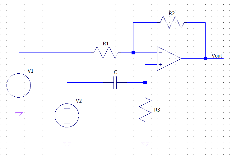
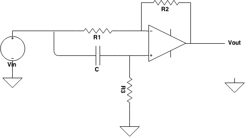
At the following circuit I want to find what it does and basically its transfer function. I've searched a lot but I didn't find any circuit like this. Since it does not match any of the basic types of op amp circuits (inverting or non-inverting amplifier) I don't know where to start from. Finally, anyone knows what's the name of this circuit? Please note that this is not homework.

enter image description here

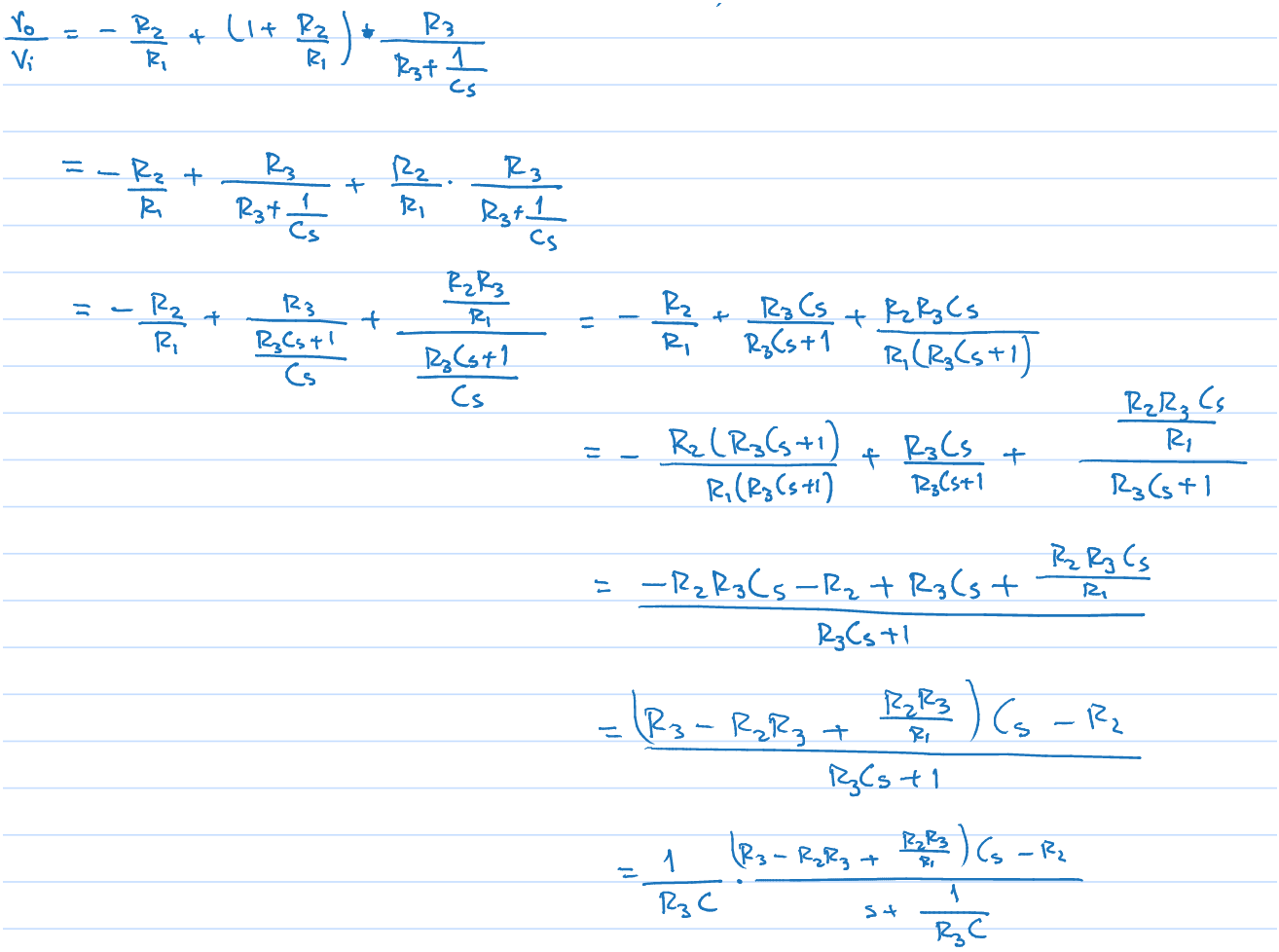
Following Lorenzo Donati's method I got to this point for the transfer function: enter image description here

\$\endgroup\$

4 Answers 4

3
\$\begingroup\$

You can determine the transfer function \$H(s)\$ of the circuit reasoning on the following circuit:

enter image description here

and thinking of \$V_1\$ and \$V_2\$ as two independent inputs. Since the circuit is linear superimposition applies, and the output (in the s-domain) of the circuit when \$V_2\$ is off is simply that of an inverting amplifier (\$R_3\$ shorts the non inverting input to ground, assuming an ideal op-amp):

\$ V_{out1} = - \dfrac{R_2}{R_1} V_1 \$

Analogously, when \$V_1\$ is off, the circuit acts as a non-inverting amplifier whose input is filtered by the series \$C-R_3\$. Thus applying the non-inverting amp gain formula and the voltage divider formula you get:

\$ V_{out2} = \left(1 + \dfrac{R_2}{R_1} \right)\dfrac{R_3}{R_3 + \frac{1}{C s}} V_2 \$

The full response is the sum of the two above:

\$ V_{out} = V_{out1} + V_{out2} = - \dfrac{R_2}{R_1} V_1 + \left(1 + \dfrac{R_2}{R_1} \right)\dfrac{R_3}{R_3 + \frac{1}{C s}} V_2 \$

Your circuit is like the one I posted, but with \$V_1 = V_2\$, therefore the full response becomes:

\$ V_{out} = V_{in} \cdot \left[ - \dfrac{R_2}{R_1} + \left(1 + \dfrac{R_2}{R_1} \right)\dfrac{R_3}{R_3 + \frac{1}{C s}} \right] \$

from which you get:

\$ H(s) = \dfrac{V_{out}}{V_{in}} = - \dfrac{R_2}{R_1} + \left(1 + \dfrac{R_2}{R_1} \right)\dfrac{R_3}{R_3 + \frac{1}{C s}} \$

This simplifies, after a bit of algebra, into:

\$H(s) = \dfrac{s - \frac{R_2}{R_1 R_3 C}}{s + \frac{1}{R_3 C}} \$

Which shows that the circuit acts as an active filter with a 1st order frequency response.

Such a topology is used, for example, to create all-pass filters if \$R_2 = R_1\$.

EDIT

The derivation of the final form of H(s) follows:

\$ H(s) = - \dfrac{R_2}{R_1} + \left(1 + \dfrac{R_2}{R_1} \right)\dfrac{R_3}{R_3 + \frac{1}{C s}} = - \dfrac{R_2}{R_1} + \dfrac{R_1 + R_2}{R_1} \dfrac{R_3 C s}{R_3 C s + 1} = \$

\$ = - \dfrac{R_2}{R_1} + \dfrac{(R_1 + R_2)R_3 C s}{R_1(R_3 C s + 1)} = \dfrac{-R_2(R_3 C s + 1) + (R_1 + R_2)R_3 C s}{R_1(R_3 C s + 1)} \$

\$ = \dfrac{-R_2 R_3 C s - R_2 + R_1 R_3 C s + R_2 R_3 C s}{R_1(R_3 C s + 1)} = \dfrac{- R_2 + R_1 R_3 C s }{R_1(R_3 C s + 1)} = \dfrac{R_1 R_3 C s - R_2 }{R_1 R_3 C s + R_1} \$

dividing numerator and denominator by \$R_1 R_3 C \$ we get:

\$ H(s) = \dfrac{s - \frac{R_2}{R_1 R_3 C}}{s + \frac{R_1}{R_1 R_3 C}} = \dfrac{s - \frac{R_2}{R_1 R_3 C}}{s + \frac{1}{R_3 C}} \$

\$\endgroup\$
5
  • \$\begingroup\$ I cannot find this function after doing some algebra. Can you check the edit I posted based on your solution? What's wrong here? \$\endgroup\$
    – mgus
    Commented Jan 1, 2015 at 23:09
  • \$\begingroup\$ Thanks, I got this. Now, is there any way to derive the Bode plot (magnitude and phase) from this function without knowing the values of the resistors and the capacitance? We know the residue and the pole but can we tell if R2/R1 is smaller or larger than one in order to see which comes first, the pole or the residue? \$\endgroup\$
    – mgus
    Commented Jan 2, 2015 at 9:49
  • \$\begingroup\$ Konstantinos - answering your question: For R1=R2 the numerator is the conjugate complex form of the denominator. From this you can derive that both magnitudes are identical and the magnitude of the whole allpass function is unity. Regarding the phase, you can start with w=0, which gives an absolute value of "-1" (phase 180deg). Similarly, for w approaching infinite the absolute value is "+1" (phase 0 deg). Hence, we have a phase function from 180 deg to 0 deg (90 deg at the pole frequency 1/C*R3). \$\endgroup\$
    – LvW
    Commented Jan 2, 2015 at 10:26
  • \$\begingroup\$ @LvW For R1=R2 and about the phase Bode plot I have an objection: as magnitude plot is a straight line at 20log(|-1|)=20log(1)=0dB from w=-oo to w=+oo, phase plot should also be a straight line at 180 degrees from w=-oo to w=+oo since the constant parameter (-1) of the t.f. is negative. Those results derive from the fact that R1=R2 which makes the pole and the residue to counteract each other. I don't understand why the phase plot should go to 0 degrees for w=+oo \$\endgroup\$
    – mgus
    Commented Jan 2, 2015 at 11:00
  • 1
    \$\begingroup\$ Konstantinos, The allpass is not a phase-minimum system (it has a zero in the RHP). Therefore, you cannot derive the phase function from the magnitude response. The phase is to be calculated using the ratio Im/Re. This gives an arctan function between 180 deg and 0 deg. \$\endgroup\$
    – LvW
    Commented Jan 2, 2015 at 12:32
1
\$\begingroup\$

Remember, ideal op amps follow two basic rules:

  1. No current flows into either input.

  2. Negative feedback forces the voltage at each input to be equal.

Let's start with a qualitative approach. Since there's one capacitor, we can divide the frequency response of this circuit into three regions -- low-frequency \$(Z_C \gg R_3)\$, mid-frequency \$(Z_C \approx R_3)\$, and high-frequency \$(Z_C \ll R_3)\$.

At DC, the capacitor acts like an open circuit, so the non-inverting input is tied to ground. In this case, the negative feedback is a simple inverting amplifier.

At high frequency, the capacitor acts like a short circuit, so the non-inverting input is tied directly to \$V_{in}\$. It's harder to see, but in this case the negative feedback gives you a voltage follower.

At mid-frequency, the frequency response transitions from inverting input to voltage follower. We expect the gain to go from R2/R1 to 1 and the phase to go from 180 to 0. This is where we have to derive the transfer function using the op amp rules. \$V_+\$ is pretty easy -- C and R3 form a low-pass filter:

$$V_+ = V_{in}\frac{R_3}{R_3 + \frac{1}{sC}} = V_{in}\frac{1}{1 + \frac{1}{sR_3C}}$$

\$V_-\$ is a little trickier, but it's mostly the same as deriving an inverting amplifier:

$$\frac{V_{in} - V_-}{R_1} = \frac{V_- - V_{out}}{R_2}$$ $$(R_1 + R_2)V_- = R_1V_{out} + R_2V_{in}$$

Now we connect our two equations with:

$$V_+ = V_-$$

$$V_{in}\frac{1}{1 + \frac{1}{sR_3C}}(R_1 + R_2) = R_1V_{out} + R_2V_{in}$$

From here, it's just a matter of algebra. It's up to you how you want to express the result, but one way that's easy to understand is:

$$\frac{V_{out}}{V_{in}} = (DC\ gain) + (AC\ gain)*(frequency\ response)$$

(Note that Lorenzo's form is probably more common in signal processing, but I like this one for educational purposes.) Here's my derivation:

$$V_{in}\frac{R_1 + R_2}{1 + \frac{1}{sR_3C}} = R_1V_{out} + R_2V_{in}$$

$$V_{out} = -\frac{R_2}{R_1}V_{in} + \frac{V_{in}}{R_1}\frac{R_1 + R_2}{1 + \frac{1}{sR_3C}}$$

$$V_{out} = -\frac{R_2}{R_1}V_{in} + V_{in}\frac{1 + \frac{R_2}{R_1}}{1 + \frac{1}{sR_3C}}$$

$$\frac{V_{out}}{V_{in}} = -\frac{R_2}{R_1} + (\frac{R_2}{R_1} + 1)\frac{1}{1 + \frac{1}{sR_3C}}$$

When s -> 0, the gain becomes:

$$\frac{V_{out}}{V_{in}} = -\frac{R_2}{R_1} + (\frac{R_2}{R_1} + 1)*0 = -\frac{R_2}{R_1}$$

When s -> infinity, the gain becomes:

$$\frac{V_{out}}{V_{in}} = -\frac{R_2}{R_1} + (\frac{R_2}{R_1} + 1)*1 = 1$$

That's the behavior we expected to begin with, which is a good sign that I did the algebra correctly. :-) You can also check with Excel or some other tool vs. what you get in CircuitLab. Doing a frequency response simulation in CircuitLab is probably the easiest way to get started with an unfamiliar filter circuit.
\$\endgroup\$
0
\$\begingroup\$

If we look at it one step at a time, R1 and R2 form an inverting amplifier with gain -R1/R2. For the non-inverting input forms a high-pass RC filter. Depending on what Vin looks like (i.e. if there is an AC and DC component) the resulting Vout will subtract the inverting input from the high pass component.

Basically this is a really poor high pass differential amplifier. I would remove C and R3 and break it out into a pre-amp stage in non-inverting configuration so as not to load the gain stage of R1 and R2.

\$\endgroup\$
0
\$\begingroup\$

Here comes the simplest way for finding the transfer function H(s):

From feedback theory for ideal opamps we know that

H(s)=-Hin/Hf

with input function (Vout=0) Hin=R3/(R3+1/sC)-R2/(R1+R2)

and feedback function (Vin=0) Hf=-R1/(R1+R2).

From this, the ratio is (after some simple manipulations)

H(s)=-Hin/Hf=(sCR1R3-R2)/(sCR1R3+R1).

Setting R1=R2 this is the transfer function for an inverting allpass (unity magnitude, phase from 180deg to 0 deg.)

\$\endgroup\$

Your Answer

By clicking “Post Your Answer”, you agree to our terms of service and acknowledge you have read our privacy policy.

Not the answer you're looking for? Browse other questions tagged or ask your own question.