0
\$\begingroup\$

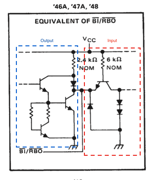
In the 7447 BCD to 7-segment decoder chip, pin 4 is BI'/RBO'. That pin acts both as input and output. I would like to understand how exactly the internal circuitry works to make this possible. On page 7 of this datasheet, there is a schematic showing the internal circuitry for the BI'/RBO' connection. Can somebody please explain how exactly this works?

Does the dashed line on the right carry the pin signal fed to the rest of the chip circuitry? If so, how can the signal there ever attain the logical "high" state? The two diodes in series will always clamp down the voltage there to be the sum of two diode forward voltages (i.e., max ~1.4V total).

\$\endgroup\$
3
  • \$\begingroup\$ Notice that the BI/RBO input side is exactly the same as the other inputs, while the output side is a weak open collector, still almost like the other outputs. \$\endgroup\$
    – Passerby
    Commented Jan 17, 2016 at 3:55
  • \$\begingroup\$ I am trying to understand how this works. Say, the pin is forced to low state from outside. When the pin is forced low, presumably the transistor on the right would conduct, and as a result, the dashed line on the right will be in "low" state; right? But, as I mentioned in my question, I don't see how that line could ever attain the "high" state since the two diodes in series won't ever let the voltage there go above 1.4 volts. Certainly, I am misunderstanding something, but, no idea where.... \$\endgroup\$
    – Victory
    Commented Jan 17, 2016 at 4:11
  • \$\begingroup\$ 1.4 Volts would be a Level High as far as the circuit is concerned. Anything higher will get clamped to 1.4 volts, and anything lower will be a Level low. Well, anything less than 0.8 V \$\endgroup\$
    – Passerby
    Commented Jan 17, 2016 at 5:04

2 Answers 2

3
\$\begingroup\$

Yes, the dashed lines show the connections to the rest of the IC.

the left half shows an open-collector output. you can't force it high without risking damage to the chip but it can be forced low, the right half represents the input circuit

see notes at the bottom of page 3

\$\endgroup\$
0
\$\begingroup\$

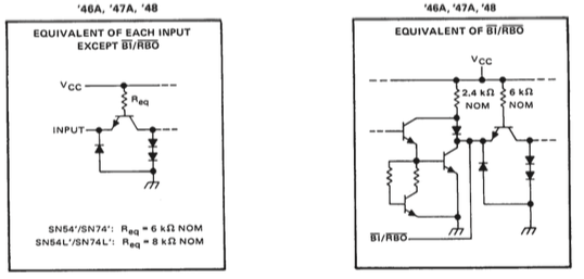
Taking a stab at this, I may be completely wrong on my reasoning. First, notice that the BI/RBO Input side is exactly like the standard inputs:

enter image description here

Yes, the dashed line on the right goes to the internal circuitry.

Now notice the Voltage Input High minimum in the specs:

enter image description here

It taks at least 2 Volts for the circuitry to be a voltage high. This is because the input uses a NPN transistor. The input is at the Emitter, while the Base is pulled High and the Collector pulled low by the 2 diodes you mentioned. When both the emitter and base are pulled a diode higher than the collector, the voltage at the floating collector is pulled high. The 2 diodes clamp the voltage down to prevent damage.

\$\endgroup\$

Your Answer

By clicking “Post Your Answer”, you agree to our terms of service and acknowledge you have read our privacy policy.

Not the answer you're looking for? Browse other questions tagged or ask your own question.