3
\$\begingroup\$

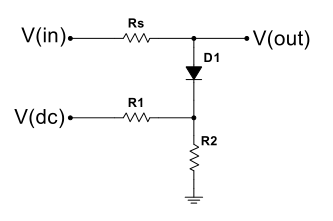
As you know a diode clamp is a circuit to protect sensitive circuits from excessive voltage. One approach to change clamping level is to use voltage dividers. most resources and textbooks represent a schematic like this:

enter image description here

and in case that diode is silicon, they compute maximum output voltage this equation: $$ V_{out} = \frac{R_2}{R_1 + R_2}V_{dc} + 0.7\space(volts) $$

as I understand we are permitted to use such equation only if Rs is very large relative to R1 and R2.

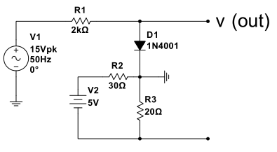
I tried to design diode clamp that limits output voltage up to 2.7 Volts. I used two approachs. first approach is this :

enter image description here

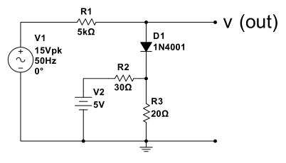
and another one is this :

enter image description here

Both approach have same result, but i want to know which one is more practical and reliable?

\$\endgroup\$
3
  • \$\begingroup\$ Both are poor methods - consider the current flowing from the 5V supply (irrespective of the input) - it's 100 mA and unacceptable to many engineers. Use an op-amp to produce 2V and not a resistor divider. \$\endgroup\$
    – Andy aka
    Commented Aug 2, 2016 at 9:28
  • \$\begingroup\$ The first should clamp at 0.7V. \$\endgroup\$
    – Antonio
    Commented Aug 2, 2016 at 9:31
  • \$\begingroup\$ This is a poor design - you have 100mA flowing through your potential divider. Voltage clamps like this are really for clamping small signals where the currents are small - not power supply applications. \$\endgroup\$
    – N.G. near
    Commented Aug 2, 2016 at 21:03

2 Answers 2

5
\$\begingroup\$

Let's start by analyzing your third circuit (the first is just a generalized concept, and the second makes no sense at all). R2 and R3 form a voltage divider. The output is (20 Ω)/(50 Ω) = 0.4 of the input. Since the input is 5 V, the output is 2 V. That's what the cathode of D1 will be at when D1 is not conducting. At this point, remember what Thevenin said and realize this is just a 2 V source with 12 Ω impedance.

Let's say the forward drop of D1 is 700 mv. That means D1 starts to conduct when its anode, which is also Vout, is 2.7 V. If we make the simplifying assumption that the diode is a fixed 700 mV voltage source when on, then its anode looks like a 2.7 V 12 Ω source when Vout is 2.7 V or above.

Any part of V1 above 2.7 V will be attenuated by the 5 kΩ and 12 Ω voltage divider, which has a gain of (12 Ω)/(5012 Ω) = 0.00239. For example, when V1 goes to 3.7 V, the part above 2.7 V will result in only 2.39 mV rise. Vin of 3.7 V therefore results in Vout of 2.704 V.

So yes, this circuit can be considered a clamp, since it greatly attenuates voltages above a certain level.

However, in most cases these circuit are not desirable. You are spending a lot of power to make the 2 V 12 Ω voltage source. The total current thru R2 and R3 even when not clamping is (5 V)/(50 Ω) = 100 mA. That is unacceptably large in many circumstances.

R2 will dissipate 300 mW and R3 will dissipate 200 mW. That rules out ordinary 0805 resistors. R2 can't even be a "1/4 W" resistor, and that would be cutting it close for R3.

Here is a better way to make a clamp using a similar concept:
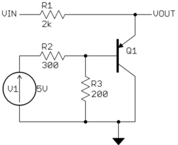
The basic difference is that the diode is replaced by a transistor. In this case, think of the transistor as a diode with gain. Current will flow thru the E-B junction like it did the diode before. However, for every one unit of current flowing out the base, there will be gain units of current flowing out the collector. The clamping current draining Vout is the total, but the voltage divider is only loaded with the much smaller base current.

In this example, R2 and R3 are 10x higher. That means they require 10x less current from V1, but also that they have 10x more impedance. However, due to the gain of Q1, the apparent impedance at the emitter is gain+1 times lower than the impedance at the base. Therefore, the transistor only needs to have a gain of 9 for this to clamp the same as your circuit, but with 10x less V1 current. Small signal transistor gains can be over 100, so in reality the resistors can be increased further and still perform as well as your circuit, but with much less quiescent current.

In a real circuit, I'd add a cap across R3. That makes the clamp even lower impedance for short term spikes.

\$\endgroup\$
5
  • \$\begingroup\$ +1 for clear explanation. Just, I think there is ambiguity or inaccuracy in explanation about impedance in last paragraph. With this we would have a higher gain at emitter, so is there a possibility that we have gain+1 time less the impedance at the base? Sorry if I didn't understand well. \$\endgroup\$
    – Haris778
    Commented Aug 2, 2016 at 12:31
  • \$\begingroup\$ @Haris: The gain of the transistor makes the emitter look like it has (gain + 1) lower impedance than the base, roughly. Approximating the B-E drop as fixed, the emitter and base have the same voltage variations. However, the current at the emitter is gain+1 higher. Dynamic Ohms is dV/dA, so lower impedance at emitter due to same dV (voltage change) but higher dA (current change). \$\endgroup\$ Commented Aug 2, 2016 at 13:31
  • \$\begingroup\$ @Olin Lathrop: there are 3 schematic diagrams in the original question. I assume that you are talking about the 2nd & 3rd schematics. Carefully examine the 2nd schematic where the ground symbols are relative to the offset voltage. \$\endgroup\$ Commented Aug 2, 2016 at 17:09
  • \$\begingroup\$ @Dwayne: Oh, I didn't notice the ground ground symbol sticking out like that in the second schematic. I'll have to update my answer, but I have to run right now. \$\endgroup\$ Commented Aug 2, 2016 at 18:36
  • \$\begingroup\$ @Olin Yes, exactly lower impedance and higher current. \$\endgroup\$
    – Haris778
    Commented Aug 3, 2016 at 7:24
1
\$\begingroup\$

The two circuits are NOT equivalent and will not produce similar results.

Note the I am assuming that you are measuring your output voltage between the two output terminals.

The first circuit clamps the input at the forward voltage drop of the diode (about 0.7V), THEN adds an negative offset voltage to the output (relative to Ground). The magnitude of the offset voltage is about 2 Vdc.

The second circuit does what you want. The output voltage is (about) the same as the input voltage until the input rises above the sum of (Diode Vf + Vdivider) or about 2.7V.

\$\endgroup\$

Your Answer

By clicking “Post Your Answer”, you agree to our terms of service and acknowledge you have read our privacy policy.

Not the answer you're looking for? Browse other questions tagged or ask your own question.