1
\$\begingroup\$

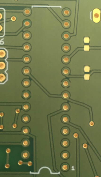
I have to solder a microcontroller that belongs to an Arduino Uno to a PCB. The Arduino uno uses the Atmega328p which has 28 pins. On the pcb I have, i see only 27 pins for the microcontroller.

Could i still somehow be able to place the 28 pin microcontroller on this PCB? Or should i make a new PCB with the 28 pins for the microcontroller?

where the microcontroller should go

Doing some research i found this footprint package: https://easyeda.com/component/ATMEGA328P_PDIP_EZ-BbicICwO6

I also never knew a 27 pin microcontroller existed or the footprint at least..

Thanks!

P.S I dont need all the 28 pins for the project.

\$\endgroup\$
14
  • 5
    \$\begingroup\$ Post a picture. First, I don't believe you. Second, if it really is as you say, I want to see that! \$\endgroup\$ Commented Dec 16, 2016 at 12:32
  • 2
    \$\begingroup\$ Vote downs should be there for the Footprint,. Not for the valid question I believe. \$\endgroup\$
    – User323693
    Commented Dec 16, 2016 at 12:53
  • 3
    \$\begingroup\$ The layout of the board seems to be a bit of a joke. \$\endgroup\$
    – Steve G
    Commented Dec 16, 2016 at 12:57
  • 3
    \$\begingroup\$ It looks like the layout was done by a 2-year-old using finger paints. I don't think I have seen anything quite so laughably bad in a long time. Can you tell us where you got that from so we can go and poke fun at them? \$\endgroup\$
    – Majenko
    Commented Dec 16, 2016 at 19:15
  • 2
    \$\begingroup\$ Is it me, or is there SOLDER MASK OVER THE ANNULARS of that footprint?!?!?!?!?! \$\endgroup\$
    – Majenko
    Commented Dec 16, 2016 at 19:16

2 Answers 2

5
\$\begingroup\$
On the pcb I have, i see only 27 pins for the microcontroller

This is very hard to believe, unless some idiot designed the board. Even if only 27 pins are actually used in a circuit, any competent board designer will put down the pads for all 28 pins. Pads are not only for making electrical connections, but also to mechanically anchor the part. Granted, holding something like a 28 pin SOIC package by 27 pins should be good enough mechanically, but there is no downside to placing all 28 pads.

If the board really only has 27 pads for your 28 pin chip, then bend up the one pin that doesn't have a pad and solder down the rest normally.

Added

Wow, that really is a 27 pin footprint for a 28 pin part! And, it's thru hole, and gold-plated. Find out who designed this and stay away from anything else he's done. The term gold plated turd seems particularly relevant here.

In the mean time, just bend up pin 28 and solder the package normally using the other 27 pins. The reason to bend up the pin is to make sure it doesn't contact anything on the board. There seem to be vias there without soldermask, so the pin could short against them. Even if the area below the pin was covered with soldermask, I wouldn't want the pin touching it and possibly eventually cutting thru the insulation. Bend up the pin, or even break it off altogether.

\$\endgroup\$
4
  • 8
    \$\begingroup\$ "This is very hard to believe" - never underestimate the Arduino effect :) \$\endgroup\$ Commented Dec 16, 2016 at 12:45
  • \$\begingroup\$ He has since added a picture. I've never anything like that before. Looks like he downloaded a component with a bad PCB footprint \$\endgroup\$
    – user103993
    Commented Dec 16, 2016 at 12:48
  • \$\begingroup\$ Whoever this idiot is, he is definitely not poor. I bet hand drawn traces look better than this. \$\endgroup\$ Commented Dec 16, 2016 at 14:55
  • 1
    \$\begingroup\$ This is exactly why I coined the name "Ardueenies"... \$\endgroup\$
    – Majenko
    Commented Dec 16, 2016 at 19:14
1
\$\begingroup\$

I was laughing a lot seeing this. Anyways, a solution could be that you solder the present lot using female headers and then insert the arduino in it and chop of the pin which is extra. And make a new PCB for the next lot.

\$\endgroup\$
5
  • 1
    \$\begingroup\$ What's the advantage of using chip sockets if you suggest to chop off the pin anyway? \$\endgroup\$ Commented Dec 16, 2016 at 12:49
  • \$\begingroup\$ Yes that's what i will do, chop the 28th pin and i should fit in. Check the footprints, 28 pins:easyeda.com/component/ATMEGA328P_PDIP-l9Fb5BvN4 \$\endgroup\$
    – ardv92
    Commented Dec 16, 2016 at 12:50
  • \$\begingroup\$ 27 pins: easyeda.com/component/ATMEGA328P_PDIP_EZ-BbicICwO6 Only difference is the 28th pin \$\endgroup\$
    – ardv92
    Commented Dec 16, 2016 at 12:53
  • \$\begingroup\$ You are absolutely right. What I meant was that he won't have to waste the PCB now that he has already got it made. For future PCBs you can use a better library with all the correct pins. \$\endgroup\$ Commented Dec 16, 2016 at 12:56
  • 5
    \$\begingroup\$ By chopping the pin of the socket atleast you won't have to severe the pin of atmega328 which you can use in your new PCB. \$\endgroup\$ Commented Dec 16, 2016 at 12:59

Your Answer

By clicking “Post Your Answer”, you agree to our terms of service and acknowledge you have read our privacy policy.

Not the answer you're looking for? Browse other questions tagged or ask your own question.