2
\$\begingroup\$

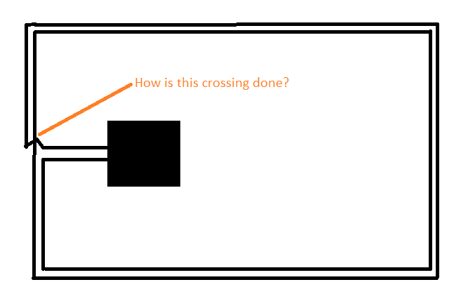
Here's a typical layout of a wireless smart card. I simplified it as far as I could. The black filled rectangle is the chip. The black lines are wires comprising the typical concentric antenna layout. I only showed two turns because that's enough to show the problem.

enter image description here

The whole assembly is then covered with plastic and turns into a plastic card which has size of a bank card - about one millimeter thick. Obviously with any concentric antenna design fitting the antenna into a thin card requires that the most outer wire crosses the other wires at some point.

As the card is being normally bent antenna wires in this crossing will have to slightly move one over another and cause abrasion of each other unless some measures are taken. So I'd guess that if I just use magnet wire and let it cross itself and put all the assembly into plastic the wire will have its insulation work out in perhaps a year or two of normal card life and the antenna gets shorted.

How is this crossing done such that antenna wires insulation survives years in a card that is being bent often?

\$\endgroup\$

2 Answers 2

4
\$\begingroup\$

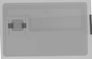
It looks like nothing special is done. See xray and other teardown.

I would say that the localised bending is probably small enough, and limited by the nearby inflexible chip, that this turns out not to be a problem. The cards do have a limited life of a few years, and although they're flexible people don't actually routinely bend them that much - the plastic itself is susceptible to bend fatigue.

\$\endgroup\$
2
\$\begingroup\$

There are basically two ways to embed an antenna in a smart card:

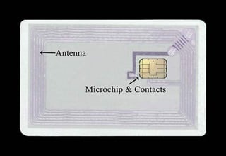
  • Either make the antenna out of enamelled wire and sandwich it between two sheets of plastic. Then, as pjc50 said, there is nothing really particular to take care of at the crossing. But this solution makes it a bit difficult to bond the antenna to the chip. There needs to be some intermediate pads between the chip module and the antenna (at least for the cards that are both contactless and also have the usual contact interface with the exposed pads).

enter image description here

  • Or build the antenna on two layers (using some etching or engraving process on a thin plastic substrate): one layer for the main track, the other for the crossing part. Then glue this together (with a particular process so proper contact is made when going from one layer to the other - it may use some conductive glue, or a machine just presses the contact points together hard enough). This makes what is called the antenna "inlay". Finally, sandwich this inlay between two sheets of plastic (and embed the chip module too):

enter image description here

(you can see the crossing section made on the other layer as the darker trace part)

\$\endgroup\$

Your Answer

By clicking “Post Your Answer”, you agree to our terms of service and acknowledge you have read our privacy policy.

Not the answer you're looking for? Browse other questions tagged or ask your own question.