2
\$\begingroup\$

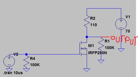
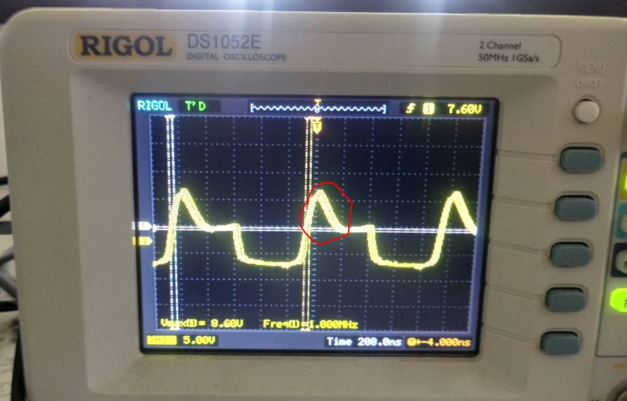
I have to make a pulse generator square wave for ultrasonic transducer with frequency 1 MHz and 70V for the amplitude, the input is function signal generator with 10V VPP output and 1 MHz. I have made it and it works, but there is a problem. There is always a ringing or overshoot in turn on or rise time but not for the fall. It happens for all frequency, not just in 1 MHz, in 100 KHz for an example, the overshoot is so tight or narrow. this is the circuit that i made

enter image description here

and this is the result of the output

enter image description here

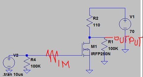
what i have done 1. try to add resistor 1M or 10K in gate of MOSFET, the result : no output signal 2. Add Decoupling capacitor, the result : no effect

UPDATE

how i add up the resistor

enter image description here

So, how to fix the overshoot or the ringing of the output?

Thank you

\$\endgroup\$
8
  • \$\begingroup\$ That oscilloscope image is without any resistor between V2 and M1, right? - How does the oscilloscope look if you put the 1 MΩ as in you described? It would be nice to see if there's any difference at all. \$\endgroup\$ Commented Nov 23, 2017 at 7:12
  • \$\begingroup\$ Hi, pal. Putting a MOSFET to 1MHz operation is quite difficult task. Anyway, what this circuit does? Where is the load? \$\endgroup\$ Commented Nov 23, 2017 at 8:44
  • \$\begingroup\$ There has to be some inductance (or an unshielded probe) to make such overshoot. The circuit as shown can't get 50V above that 70V rail. Reroute the probe wiring, and put a second probe on the power supply. \$\endgroup\$
    – Whit3rd
    Commented Nov 23, 2017 at 9:48
  • \$\begingroup\$ Gate drive R of about 10 Ohms to damp ringing. | Small Schottky diode across FET gs as near as FET as possible. Cathode to gate so diode conducts when gate goes negative. Ringing gate has negative excursions clamped. | Zener gs - Vzener > V2 and usefully less than Vgsmax. | Small ferrite bead on source lead - getting desperate. | Is R2 inductive? \$\endgroup\$
    – Russell McMahon
    Commented Nov 23, 2017 at 13:54
  • \$\begingroup\$ @HarrySvensson , there is no any signal if i put the 1 MOhm resistor series with the gate \$\endgroup\$
    – Zahi Azmi
    Commented Nov 24, 2017 at 3:00

3 Answers 3

5
\$\begingroup\$

what i have done 1. try to add resistor 1M or 10K in gate of MOSFET, the result : no output signal

You've done that what you shouldn't do! If you check the datasheet then you'll see that the input capacitance, \$C_{iss}\$, is quite high: 2.16nF. A 1M gate stopper resistor plus this capacitor will form a nice low-pass filter having a cut-off frequency of \$f_C=1000/(2\pi \cdot 2.16 \cdot 1) = 73.7Hz\$, so the input pulses will be totally chopped off thus the MOSFET will never turn on. That's why you get no output.

Cure: Remove 100k and change 1M to a resistance so that it forms a LPF having a cut-off frequency of at least \$3 \cdot f_{SW} = 3MHz\$.

  1. Add Decoupling capacitor, the result : no effect

Of course! Any inductance causes ringing. Where do you have inductances? Answer: Cables and internal drain inductance of the MOSFET.

Cure: A snubber network across Drain and Source/GND. You can find a lot of info about snubber design on Internet.

PS: Your MOSFET does not seem to be suitable for switching at 1 MHz. You should use another like this one (I picked this one randomly. You select according to your voltage and current needs).

\$\endgroup\$
2
  • \$\begingroup\$ the 100K resistor, is it the parallel one? and should i add a series resistor before the gate? \$\endgroup\$
    – Zahi Azmi
    Commented Nov 24, 2017 at 3:03
  • \$\begingroup\$ Yes, remove that parallel one. As for the series gate stopper resistor, although you cannot use any higher than even 1 ohms because of the high input capacitance of the MOSFET, if you really want to put a resistor then its value should be calculated from \$3MHz = 1/(2 \pi \cdot R \cdot 2.2nF)\$. \$\endgroup\$ Commented Nov 24, 2017 at 3:53
1
\$\begingroup\$

Layout is very important to reducing ringing in gate voltage. You want to optimize for low inductance on the gate drive trace. So think short traces thicker traces can also help with this a bit. The other part of reducing gate ringing is slowing the transition time down which is what the other comments/answers are trying to accomplish with the resistors.

It could also be a measurement artifact if you are not using the ground spring clip on your scope

\$\endgroup\$
1
  • \$\begingroup\$ This is definitely an answer. \$\endgroup\$
    – pipe
    Commented Nov 23, 2017 at 14:30
0
\$\begingroup\$

I just wanted to add that there will be some inductance between the power source and the drain of your MOSFET (and also on the return side). Remember that the faster you switch the load and the larger your current, the larger the voltage spike you'll see.

$$V = L\frac{di}{dt}$$

Where V here is the voltage across your parasitic inductance. Wide traces should be used with heavy weight copper if you're switching large loads quickly.

This voltage will appear in addition to your source voltage (70V). Less resistance in series with the gate will cause faster switching and more resistance will cause slower switching. Keep in mind the gate of the MOSFET will need a gate driver if you want to switch loads very quickly and reduce power dissipation in the FET. In addition to reducing the inductance at the MOSFET drain, you should also try and keep the loop distance small connecting you power sources positive and return terminals.

\$\endgroup\$

Your Answer

By clicking “Post Your Answer”, you agree to our terms of service and acknowledge you have read our privacy policy.

Not the answer you're looking for? Browse other questions tagged or ask your own question.