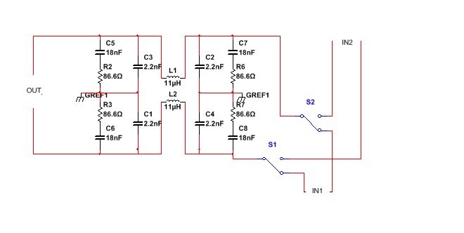
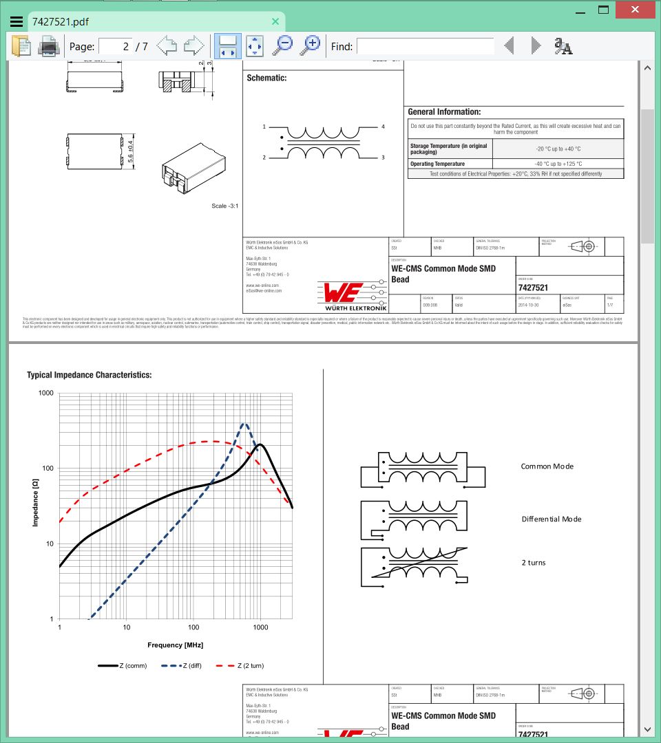
I am working on a project with two inputs and an output as shown. IN2/OUT are external connections, and IN1 is internal. Based on input from this forum and research I have come up with the following common-mode filter for placement between IN2 and OUT. (L1&L2 are actually the same CM choke, just drawn separate.)
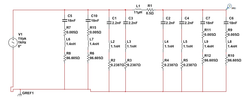
 I've calculated and simulated this as shown:
I'm happy with both differential and common-mode response, but I've only simulated the filter in common-mode without any load, as I don't exactly know what to use for a load when simulating CM filters. So my questions:
1) Does this topology look ok with the way the circuit is supposed to function (shunting CM cable noise from IN2 and OUT out of the circuit?
2) When simulating CM filtering, what is usually used as a load? I watched a youtube video where a current source was used to simulate the filter, but I didn't fully understand the reasoning behind it.
3) This may be a brain fart question, but is there any useful significance to simulating filter frequency response without any kind of load, since the source and load will change the frequency response? I was reading a post about PI filter analysis, where differential filter response was said to be meaningless without source and load attached.


