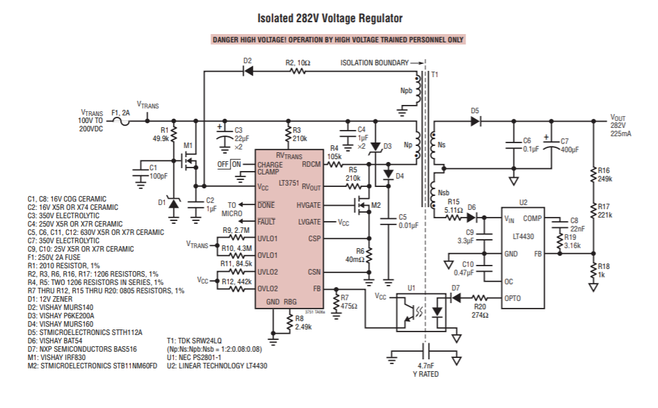
The larger design is for a 170 V input, 500 V 2 mA output using a flyback converter. I will refer to the schematic on page 29 of the LT3751 switching controller, also found below.
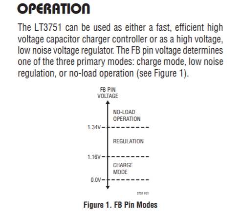
The feedback pin of the switch controller controls the mode of operation: CHARGE MODE, REGULATION, NO LOAD (Fig 1 page 10 LT3751), also included below. I wish to avoid exceeding 1.34 V on this pin as that pushes it into NO LOAD, and the output voltage can increase up to 10% above nominal (page 14 LT3751).
Using the Isolated 282 V Voltage Regulator on page 29 LT3751, wouldn't this result in the voltage on the LT3751 switching between 0 V and Vcc?
If this is the case, how can I avoid this? I wish to operate in REGULATION mode. Is there a analog optocoupler type device, like a isolated operational amplifier what would pass the voltage sensed between R17 and R18 to the LT3751 FB?
Note the FB pin is internally regulated to 1.22 V (page 8 LT3751), so it would be acceptable to apply a voltage between 1.16 V and 1.22 V when the output is low, and between 1.22 and 1.34 V when the output is high. How could I achieve this using the optocoupler? Also, would the optocoupler present any significant resistance itself into a voltage divider circuit (ON/OFF).


