0
\$\begingroup\$

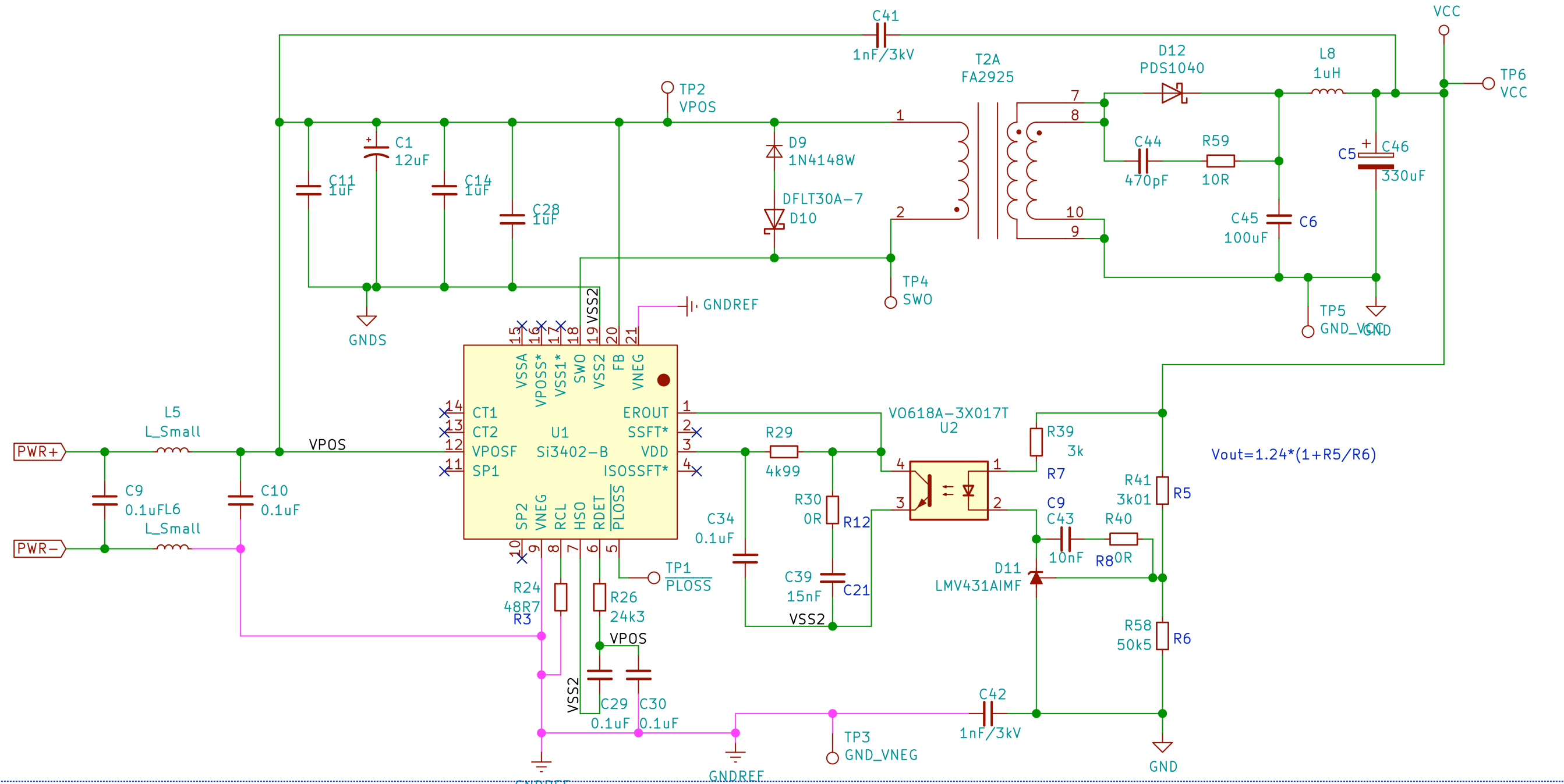
I am currently designing a PoE device with IC Si3402B Isolated refer and circuit my design:

enter image description here

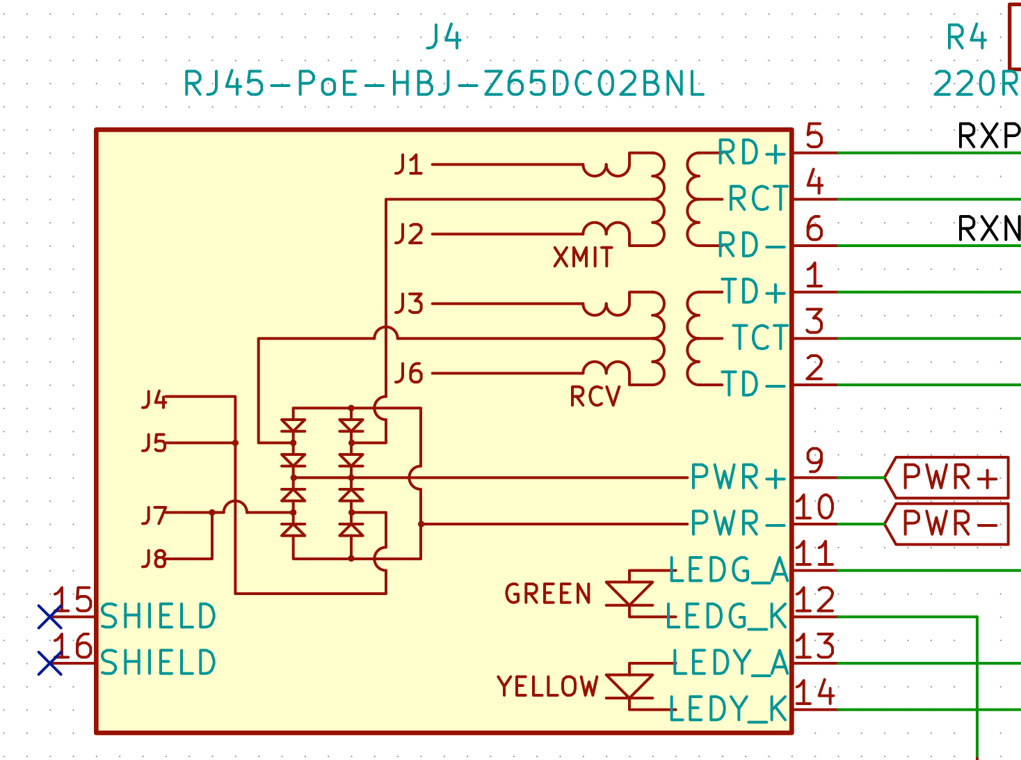
I use an RJ45 port with an internal diode bridge:

enter image description here

I bought the RJ45 but not yet. I tested the external power supply from the 51VDC-1.25A adapter to supply directly to the PWR+ and PWR- power sources. But the circuit does not work and the Si3402B chips heat up very fast.

As far as I understand, the power from the RJ45 will be the same DC voltage as the adapter. Is it true ?

I do not know where I was wrong. Please help me find the wrong point in the circuit I design?

I am a new member, if anything is not accurate, please help me know about it.

Thank you.

\$\endgroup\$
3
  • \$\begingroup\$ sorry about that comment glitch. 2nd part never made it for some reason. R5/R6 in your schematic indicate a 1.32VDC output, but your flyback is a 1:1, so the PWM is likely going to be having a tough time, or is this an error? For a class 3 PD (based on your R24 value the Si3402B requires at least one of the CT and SP pins to be powered by the PSE lines, but looking at your RJ jack part, I don't know if it will work because normally the CT and SP pins would be biased a diode drop higher than the bridge output. \$\endgroup\$
    – user201365
    Commented Oct 18, 2018 at 3:10
  • \$\begingroup\$ Carefully read AN956 and the Si3402BISO-EVB documents before making changes to the design like this, it's easy to miss critical stuff. Also make sure your PCB layout meets their thermal resistance guidelines and that the thermal pad is connected to the proper netlist node. \$\endgroup\$
    – user201365
    Commented Oct 18, 2018 at 3:10
  • \$\begingroup\$ Hi @isdi, As you say, my point is wrong at R5 / R6. I have corrected the + replacement diode to match the voltage out and it was running. And the SI3402B IC is not half hot. Thanks you. \$\endgroup\$
    – Duc Trinh
    Commented Oct 18, 2018 at 9:23

2 Answers 2

0
\$\begingroup\$

Move to answer from comments:

R5/R6 in your schematic indicate a 1.32VDC output, but your flyback is a 1:1, so the PWM is likely going to be having a tough time, or is this an error? For a class 3 PD (based on your R24 value the Si3402B requires at least one of the CT and SP pins to be powered by the PSE lines, but looking at your RJ jack part, I don't know if it will work because normally the CT and SP pins would be biased a diode drop higher than the bridge output. – isdi 10 hours ago
Carefully read AN956 and the Si3402BISO-EVB documents before making changes to the design like this, it's easy to miss critical stuff. Also make sure your PCB layout meets their thermal resistance guidelines and that the thermal pad is connected to the proper netlist node.

\$\endgroup\$
0
\$\begingroup\$

I had bad luck designing PoE despite a lot of effort. The problem is that there is a lot of standards for PoE (2 main), using different wires on the cable, and that from my experience a lot of product doesn't even follow the standard or are out of spec.

You should read first the PoE standard and then check which standard this chip is using.

PoE has a fairly complex startup and timing limitation in power draw and you can't just hookup a standard power supply, you need a proper PoE supply, with the standard that fits your chip.

You can see the power-up sequence on Figure 5 of the datasheet.

\$\endgroup\$
1
  • \$\begingroup\$ There are a couple of items, but I need some more information: \$\endgroup\$
    – user201365
    Commented Oct 17, 2018 at 18:01

Your Answer

By clicking “Post Your Answer”, you agree to our terms of service and acknowledge you have read our privacy policy.

Not the answer you're looking for? Browse other questions tagged or ask your own question.