Before even getting to the calculation part, it's important to point out that you've mixed up stray capacitance (what you would use for snubber calculations in this case) with interwinding capacitance (which is totally irrelevant for determining your snubber values).
While interwinding capacitance does play a role in what kind of harmonics are conducted back into mains, but that's a totally different concern and not a factor in calculating snubber component values. The only way for your bridge rectifier to see this capacitance is if it was connected the same way as you measured it - across the primary and secondary. But they're not - they're connected across the secondary. They're connected to one terminal of this parasitic capacitor, but the other terminal is floating as far as anything purely referenced to the secondary side is concerned.
What is important is the stray capacitance, which is parasitic capacitance formed across the two secondary leads. Physically, it is the capacitance formed between the windings of one coil to the other windings to that same coil. The capacitance is there, even if it has a fairly low value resistor shorting it (the secondary winding resistance).
With that out of the way, snubbing only has one thing with an 'optimum value', and I think it is beneficial to get a conceptual understanding of what is even going on, as it makes all of this stuff a lot easier to understand, and actually reduces (!) the math you need to worry about.
A Moment to Reflect
Before one can understand a snubber, one must understand the snubbee. The thing being snubbed. This is, of course, ringing.
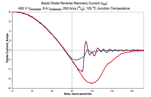
Ringing is caused by reflections. In transmission lines, and or hitting something with a hammer, or any energy flow. When a sudden discontinuity in the characteristic impedance of a current path, it results in some of that energy getting reflected back towards the source. And a diode, transistor, relay, or other switching element represents more or less the worst possible case of discontinuous impedance - it goes from being the characteristic impedance of that leg of the circuit to effectively infinite (save for a trickle of leakage current) and often in a matter of nano seconds.
This is bad. That is going to cause a significant reflection. Reflections contain meaningful amounts of energy, and this energy isn't going to just disappear, it is going to slosh around in whatever will store it until dissipated. And what will store it? The parasitic capacitances and inductances of our circuit of course!
Together, they form an LC tank, oscillating at the resonant frequency as determined by the amount of parasitic inductance and capacitance making up the tank. This is the source of the ringing, and what determines the frequency it rings at.
Reflections in the context of transmission lines and characteristic impedances can get confusing because this is all very abstract. All you need to understand it however is to understand that the word 'reflection' is not being used metaphorically. These are actual reflections! The kind you are quite familiar with already: the reflection from a piece of glass, the echo off a rock wall, or the heat reflected off the parabola of a heat lamp. Vibration in a chime struck against a wall. This is all we are talking about, and it is common to any movement of energy. Don't let the more abstract quality of this otherwise familiar occurrence through you off - you already understand reflections in transmission lines, but might not realize yet that you do.
Stop, Hammer Time
Understand that what I am about to say is more just an analogy, but a mechanical equivalence of the same effect.
Imagine that the current flowing through the diode (in the reverse direction - it is still the recovery period and the diode hasn't had time to 'turn off' or block the reverse flow yet) is a hammer that you're swinging through the air. There is a small resistance to your hammer swing in the form of air resistance. This is the characteristic impedance. It's the impedance you expect to feel at every point along the swing. However, once the diode slams shut, this is a sharp discontinuity in impedance, one that results in a huge increase of impedance. This is your hammer hitting a hard surface. It brings your swing to a halt, but this doesn't remove all the energy from this situation. Some of the energy of your hammer blow is reflected back into the hammer, causing it to bounce and vibrate (ring) in your hand. It dissipates quickly though, usually in the form of heat - the hammer head will begin to heat up after blow after blow. This is because some of the energy of each swing is being reflected back into the hammer, and this occurs because of a change in mechanical impedance - from moving through air to suddenly encountering a hard barrier, or even just splashing into water.
That's all that is going on, even if it all happens invisibly in the circuit.
With that in mind, the snubber is simply a way to dissipate some of that reflected energy as heat - just like with the hammer. The hammer is already well-snubbed by the steel it is made out of, but our circuit is not a hammer, it is more like a chime. It rings for a long time and loudly after being struck, so our snubber is like placing your hand on it to end the vibration quickly.
Math Time
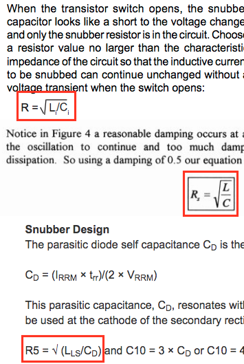
OK, we're actually getting to the answer part! Armed with this conceptual understanding, let's talk RC snubbers. The part about an RC snubber that we actually need to calculate and pick an optimal value for is the 'R' of the snubber. You might have guessed what we are trying to do here already: provide a resistive path that matches the characteristic impedance of the circuit in parallel with the switch. This is simply equal to the impedance due to the parasitic capacitance and inductance (the same thing that also causes the LC tank and the ringing). Which is, of course:
$$
R=\sqrt{\frac{L}{C}}
$$
I would note that in all 3 articles you linked, they all give the same formula, this formula.
This is the important part. If we don't match the impedance of the rest (reactive) component of the circuit, then we will still have the same problem with reflection and our snubber won't do much good, or can even make things worse.
However, if we just put that resistor in parallel with our switching element... we won't be switching much of anything anymore. There is an entire alternative path now and a diode is made irrelevant in this way. So we add a capacitor in series with the resistor to block DC current from flowing, allowing our switch to actually do something useful.
Now, instead of energy getting reflected back towards the source (and into the parasitic tank formed by the capacitance across the diode and the inductance of the transformer secondary and any other parasitics at play), it can continue on smoothly through the same impedance it had been in the form of our snubbing resistor, R, and into our snubber capacitor. The capacitor at a minimum needs to be equal to the parasitic capacitance so it can actually absorb this energy without causing a reflection. The capacitor itself doesn't snub anything, it is merely there to give it somewhere to go that requires going through the resistor, R. The only component that is actually snubbing - or dissipating - this energy is the resistor, R. The imaginary component of complex impedance - reactance - is impedance caused by storing of energy, vs. the real component, which is caused by the dissipation of it. We want to dissipate, not store this energy, and our snubber gives the energy a dissipative path it can go through, reflection free (mostly), when our diode or whatever slams shut like brick wall.
However, the resistor won't dissipate all of it immediately. Some still gets stored in the capacitor, and it still gets released back and the ringing will still be there, but the peak amplitude as well as how long it takes to subside will be much less, thanks to now being forced to move through our dissipative element, R, instead of just sloshing around in an LC tank with only the poorly-matched impedance of our secondary winding's resistance to ineffectively dissipate it.
Increasing the resistor value will not allow all of it to flow into our snubber capacitor and get reflected back, and less will not dissipate as much of it as we could be, so this really is the one value here that has an optimum value that we need to pick carefully.
The rest doesn't really matter very much.
Ok, it does, but not in the way you probably think. Remember, the capacitor stores energy, it is doing nothing to help dissipate this leftover energy from the diode turning off.
There is no optimum value for the capacitor, beyond that it needs to be greater than the parasitic capacitance across the switch we're snubbing as this ensures that there is room for all of the reflected energy on the other side of the resistor, so it will all flow through the resister, maximizing the dissipation we get.
It does have a more subtle effect however. Let's look at the resonant frequency of this ringing:
$$
f=\frac{1}{2\pi \sqrt{LC}}
$$
There is no 'R' in it. Our snubber resistor doesn't change the frequency, but when the diode/switch/whatever is off, our snubber capacitor is in series with the inductance and capacitance we're snubbing. It's now part of the LC tank, and that means the ringing frequency is going to change. Again looking at the resonant frequency equation, we can see that quadrupling the capacitance will reduce the ringing frequency by half. In other words, if we pick a C that is 3 times that of our calculated parasitic capacitances, it will cut the ringing frequency by a factor of 2. This means that it will take twice as long for the reflected energy to flow through our dissipating snubber resistor, and that much more energy (and more power, being energy over time) will be dissipated in the resistor.
No Answer, No Cry
Why not just make the capacitor huge? It's a trade off. An ugly one. will increase the dissipation demands on the resistor and lower efficiency, or at the extreme, waste excessive amounts of power and needlessly load the transformer and begin to approach the original problem with just using a resistor by itself and remove the solution provided by using a capacitor in series in the first place.
The RC snubber has an RC time constant like any other RC series circuit. This needs to be small relative to the on time of our switching element - otherwise it's little different than simply having a resistor shorting out or switch. The on time for a bridge rectifier, assuming 50Hz mains, this would be half the period of 50Hz, or 10ms. The snubber is going to do its thing when the switch is on or off, and the closer the time constant gets to our on time, the more power we'll waste filling that capacitor and dissipating energy that wouldn't ordinarily be part of the reflection.
This is a rule of thumb, but you ideally want the time constant of your snubber to be less than 1/10th the on time of your switch, so 1ms in this case. But don't just jump straight to this value either - you'll be placing a lot of extra load on the transformer, dissipating a lot of heat, and for very little real benefit. And 1/10th is somewhat arbitrary, and represents a reasonable maximum before the tradeoff has reached silly extremes.
The trade off is up to you, the articles you linked give you everything you need, especially the first one, which goes through the practical considerations of the trade off, such as power dissipated in the resistor and switches. It also gives a very good rule of thumb, which is identical to the rule of thumb in the maxim article, which is simply to not worry that much and pick a value equal to 3 or 4 times the parasitic/intrinsic capacitance of the LC tank. Rules of thumb exist because they give a good balance in a trade-off situation that generally work well for any situation where you don't really need to care that much about the trade off. Unless this is going to be a 1000W amplifier, you probably don't need to care. But minimally, you need the capacitor to be equal or greater than the parasitic capacitance, as this is the minimum needed to store all the energy that will be stored in the inductance.
And there are even caveats with the resistance: while there is an optimum value for snubbing out that reflected energy as fast as possible, it is not the optimum value if you care more about, say, the peak voltage that results. If you need to prevent this from overshooting the value of something voltage-sensitive like a MOSFET (which might have a breakdown voltage near the voltage they're switching, unlike bridge rectifiers that often have a break down an order of magnitude or more greater than the voltage they're blocking), then you actually will often select an R that is very much sub optimal, less often less than half the value. Your ringing will be worse but lower in amplitude.
I disagree that the articles give different ways of calculating anything - they all give the same formulas as near as I can see:

Its sounds like you're hoping for a simple equation for R and C that will just tell you the best snubber to make, but that isn't going to happen because the problem can't be reduced to that. I've told you how to find the best R, and 'best' strictly in the sense of snubbing as much of that reflected energy as possible and in no other way. There is a useful range of capacitances, but the exact value is a trade off with other considerations that are up to you to figure out (or not, and merely use the rule of thumb - which is what I would suggest). And if you are less concerned about noise and more concerned with the peak amplitude, then the 'best' resistor is actually a very poor choice.
Which is why I spent so long answering a question you didn't ask - what is actually going on here, because that's what you need to understand to navigate this problem space. And it doesn't just apply to snubbers, it can come in handy over and over again in a variety of different design situations.


