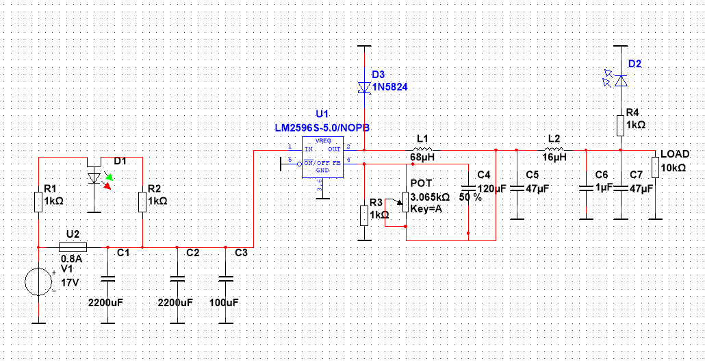
I have to reverse engineer a PCB of a buck converter and figure out the component values. Given is that Vin = 15-20V and output is 5V @ 1.5A. The converter is LM2596, and datasheet I used is found here. http://www.ti.com/lit/ds/symlink/lm2596.pdf
I have constructed a schematic and read up on components that are on board as can be seen below

I tried breaking down the components and the reasons why they are present on the board. Current component values are not correct. First thing that confused me was R1 and R2, because it seems to me that fuse should be in series with everything that comes after the power supply, so in case of malfunction it pops and divides the power source from the rest of the circuit. Is there any reason why it is put in parallel? Do resistors create open circuit or a short when they burn, or can it be both?
Next question is regarding input stage of the chip: I gathered from the datasheet that there is one input capacitor, to smooth out current spikes from power source and protect the chip, however, what is the purpose of C2 and C3? I found online that it could be to filter out low/high frequency noise, but is it applicable if the source is DC?
Regarding output stage, I wanted to know if the potentiometer is in the feedback loop to adjust the phase compensation for output?
Also, and this is the last question, why are there 3 output capacitors? I understand that C5 would be smoothing capacitor to reduce ripple voltage, but what would C6 and C7 serve? Do these have something to do with noise from switching in the chip itself?
Any explanations or directions to useful materials would be appreciated!
