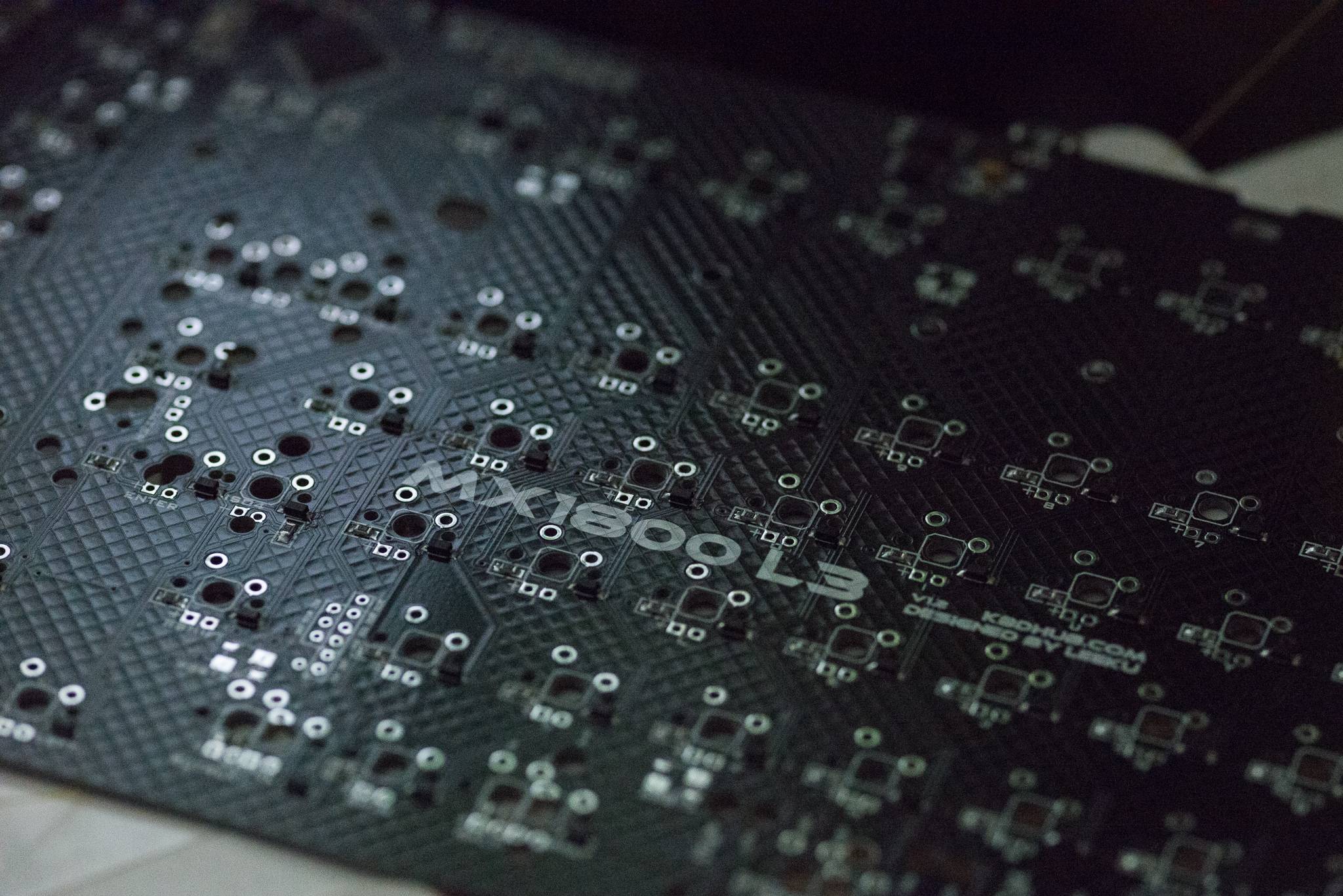
In the example image below the pcb is shown to have a textured honeycomb like mesh texture on the solder mask. My question is how would one go about creating a textured finish to the PCB like seen in this picture below?
-
3\$\begingroup\$ That may be the top copper layer showing through the solder mask. \$\endgroup\$– Mattman944Commented Jun 10, 2019 at 0:24
-
3\$\begingroup\$ that is not a solder mask, it is copper .... if you look carefully you will see that the signal traces and the grid are raised by the same amount \$\endgroup\$– jsotolaCommented Jun 10, 2019 at 1:07
1 Answer
The pattern is on the copper layer. It appears they have used the "hatched" pour option in the PCB design software with an unusually low fill. You can see the regular pattern of the pour being broken up by tracks and one area where the pattern is missing completely, presumably because the "remove dead copper" option was used when making the pour.
It looks different from normal because the solder-mask is an opaque black rather than the normal translucent colors. So while on a normal PCB you see a color difference between copper/non-copper areas here you see only the texture.

