1
\$\begingroup\$

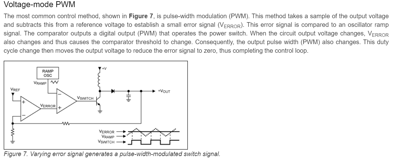
The following description is taken from maximintegrated website (this link specifically), and after reading and trying to analyze the control technique it still does not make sense to me:

1 - In the figure it shows a boost converter, and it reads:

This duty cycle change then moves the output voltage to reduce the error signal to zero, thus completing the control loop.

From my point of view if that \$V_{ERROR}\$ is supposed to converge to zero for a steady state output voltage, the duty cycle should be kept steady at 0% since \$V_{RAMP}\$ will always be greater than \$V_{ERROR}\$ and the latter seemingly not subject to variations, which cannot be true since it meant the circuit would stop switching. A comparison I have used to understand it better is when I think of a PI controller, which brings the error to zero but has a memory in its output value, so it only responds to small variations once the steady state value is reached.

enter image description here

My question is: How is this control loop supposed to keep the output voltage steady regardless of for instance, load variations, if the error being reduced to zero would actually stop the switching?

By the way in the timing diagram they've inverted \$V_{SWITCH}\$ since it should be high when \$V_{ERROR} > V_{RAMP}\$, but it does not matter to the main question since it must've been a little mistake.

EDIT:

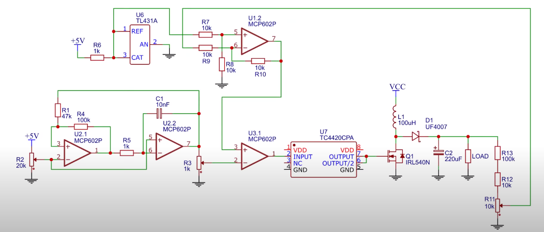
Following the main discussion, the figure below shows the circuit I have been inspired from to get this control loop done. It comes from this video in which the designer himself references maximintegrated's website.

enter image description here

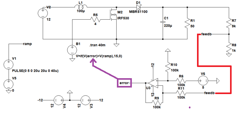
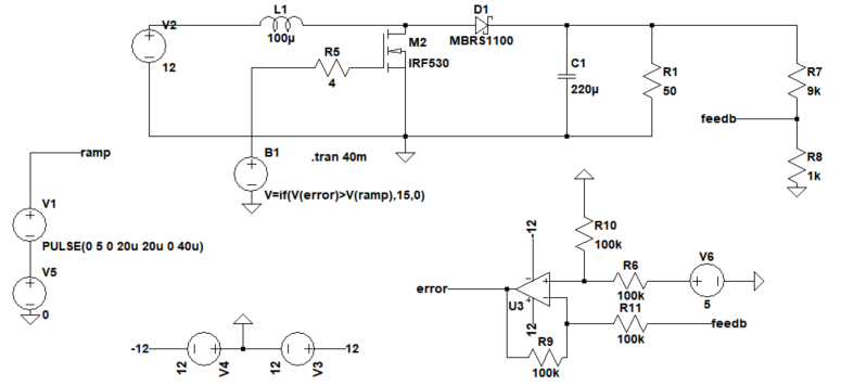
I tried to replicate the idea using an op-amp, a behavioral voltage supply and a pulse source to generate the triangular wave in LTspice, trying to replicate the idea described in maxim's document and here are the results.

enter image description here

enter image description here

I have set a value of \$V = 5\,V\$ which is the reference for \$ 50\,V \$ in the output since \$V_{feed} = 0.1\,V_{out}\$.

Result: As you can see, my voltage level in the output is \$V_{out} \approx 25\,V\$, which is not what I have set the system for. Also, I tried changing values of the load and the output voltage also changes and that's not what I wanted either.

Finally, I'm probably mistaken in how this controller works and would really like to find out what is wrong.

Thank you in advance

\$\endgroup\$
8
  • \$\begingroup\$ I suspect that "the error signal" doesn't mean \$V_{ERROR}\$ but instead \$(V_{in-} - V_{REF})\$...Actually, maybe I'm wrong, those should just be the same but with a multiplication by the gain. Maybe they're assuming positive and negative supplies on the opamps but you're thinking single supply? So \$V_{ERROR} = 0\$ is actually in the middle of the ramp, which can go negative? \$\endgroup\$
    – Justin
    Commented Feb 10, 2021 at 19:24
  • \$\begingroup\$ @Justin I thought like that so, but it may be very misleading if that's the point, at least in my point of view. I've seen a guy work a circuit with such feedback and it would work. \$\endgroup\$ Commented Feb 10, 2021 at 20:38
  • \$\begingroup\$ The schematic as shown is not inherently stable as the LCR ratios affect Q, the startup power maybe is outrageously greater than the design full load. There is no PFM soft start nor any lead/lag compensation nor any proper gain control. It can be made to regulate, but stability is not to be assumed. \$\endgroup\$
    – D.A.S.
    Commented Feb 10, 2021 at 23:24
  • \$\begingroup\$ Based on some of your comments on answers, I think the problem is you are assuming that zero is not the halfway point of the ramp. The ramp is centered around 0.0V, going to negative voltage half of the time and positive the other half. \$\endgroup\$
    – Justin
    Commented Feb 11, 2021 at 15:20
  • \$\begingroup\$ @Justin Exactly, but I've seen it be made with a ramp going from 0 to a +V being V>0, which I don't see making much sense without compensation. \$\endgroup\$ Commented Feb 11, 2021 at 19:14

4 Answers 4

3
\$\begingroup\$

How is this control loop supposed to keep the output voltage steady regardless of for instance, load variations, if the error being reduced to zero would actually stop the switching?

Basically, and in a nutshell, the error cannot reduce to zero. In a practical controller, the open loop gain may be numerically a thousand to 1 million so, if the output is (say) at 50 % of its range, then the error signal magnitude is a tiny fraction of 1 %. There has to be an error (no matter it being small), that drives the output to very, very close to the demanded level.

Exactly the same story for an op-amp; we say that both inputs are at the same voltage but that isn’t, strictly speaking, the precise truth.

And, in addition, if I address this point: -

the error being reduced to zero would actually stop the switching?

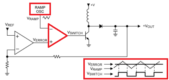
No it wouldn't because of the comparator and triangle wave shown below. They ensure that the system remains clocking out at the required duty cycle: -

enter image description here


Regards your simulation, now that I've had a good chance to look at it, you haven't got enough "gain" in the system to drive the error towards an acceptable value: -

enter image description here

Your error amplifier is only a gain of unity so, try adding a gain of ten stage between the op-amp output (U3) and the purple error box shown above. If things start to look unstable you might need a few pF across R11. If OK, proceed to increase the extra gain factor higher and higher. As you do so, the actual output will move ever closer to the target demand.

\$\endgroup\$
1
  • \$\begingroup\$ Comments are not for extended discussion; this conversation has been moved to chat. \$\endgroup\$
    – Voltage Spike
    Commented Feb 13, 2021 at 5:42
1
\$\begingroup\$

A comparison I have used to understand it better is when I think of a PI controller, which brings the error to zero but has a memory in its output value, so it only responds to small variations once the steady state value is reached.

That is indeed how the control circuit of a switching converter generally works. The diagram in your question does not accurately show this. However, the next diagram in the tutorial helps a little.

enter image description here

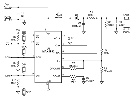
Pin 8, in that diagram is connected to a resistor, capacitor pair, and these provide the "integral" part of the control.

If we go to the datasheet for the MAX1932 figure 1 page 10, we can see that the "comp" (compensation) pin, is connected to the Verror signal. So this signal is "integrated" (or at least "stabilized") before being fed into the ramp comparator. This is typical of how switching converters work. (There are some chips that do not provide a pin for external control of compensation.)

My question is: How is this control loop supposed to keep the output voltage steady regardless of for instance, load variations, if the error being reduced to zero would actually stop the switching?

In the absence of compensation, a given error signal will cause a given duty cycle to be generated. If the given error signal is "zero", some particular duty cycle will be generated. That duty cycle will not be zero, nor 100%, but somewhere in the middle. If the error signal goes positive or negative, the duty cycle will become greater or smaller appropriately.

Let's call the duty cycle generated by a zero error signal \$D_0\$.

Let's call the output voltage for which the converter is designed \$V_0\$

If a duty cycle of \$D_0\$ causes the converter to output \$V_0\$, then the error signal generated by the output will also be zero. The converter can possibly be stable at this point.

If a duty cycle of \$D_0\$ causes the converter to output a voltage different from \$V_0\$, then the circuit will not be stable at its designed output voltage. There might be a stable point very near the designed output voltage. Alternatively, the output voltage may oscillate around some point near the designed output voltage. The compensation referred to previously is intended to stabilize the circuit, and prevent such oscillations.

\$\endgroup\$
7
  • \$\begingroup\$ It's exactly this stable point very near the designed output voltage that my circuit is not being able to converge, and I've assembled the circuit just like it was done in maxim's website. For me it's weird because if there is not an integrator taking part of the control loop, I don't see how the circuit will actually converge, although there's lots of explanations of this mode on the internet. \$\endgroup\$ Commented Feb 11, 2021 at 20:09
  • \$\begingroup\$ Moreover, I have just updated the additional information about the circuit. \$\endgroup\$ Commented Feb 11, 2021 at 20:10
  • \$\begingroup\$ OK. I think I know what is going on. In the video, he demonstrates a falling voltage when (what looks like) a 1/4 watt resistor is added as a load. From this, I conclude that the boost converter is operating in discontinuous conduction mode (DCM). The control mechanism is different in DCM than in CCM, DCM is entered when the load is "light", in relation to the L (and C?) of the converter. In your schematic, you have a 50\$\Omega\$ R1, What happens when the load resistance is increased, to say 1K? What is your output voltage then? \$\endgroup\$ Commented Feb 11, 2021 at 20:32
  • \$\begingroup\$ I have changed R1 to 1k and now the output voltage reaches a steady state value of 40V in 240ms \$\endgroup\$ Commented Feb 11, 2021 at 20:44
  • \$\begingroup\$ So maybe my circuit is not working in DCM like his? That's something I hadn't thought about to be honest. Yet I still don't understand how my circuit could not follow the idea presented by maxim's document. \$\endgroup\$ Commented Feb 11, 2021 at 20:47
1
\$\begingroup\$

The reason why the following circuit does not output 50V lies with the values of the resistors, the reference voltage and the set points of the triangle wave.

enter image description here

When the circuit is first started, the \$V_{out}\$ does pass through 50V. At that point, \$V_{fb}\$ is approximately 5V, and \$V_{err}\$ approximately 0V. So, the duty cycle is approximately 0, and so \$V_{out}\$ would fall (if there were no excess energy in the LC components).

When \$V_{out}\$ falls to approximately 25V, \$V_{fb}\$ is approximately 2.5V, and \$V_{err}\$ is approximately 2.5V, and the duty cycle will be about 50%. The output corresponding to 50% when \$V_{in}\$ is 12V, will be 24V. So the output should still fall but not by much.

The equations we have are

\$V_{out}=\frac{V_{in}}{1-D}\$

\$V_{fb}=K_{fb}V_{out}\$

\$V_{err}=V_{ref}-V_{fb}\$

\$D=\frac{V_{err}}{V_{triangle}}\$

There are multiple ways to get a 50V output. The easiest way is to adjust \$K_{fb}\$ so that, working backward, we get 50V. Notice that in the video from which the OP modeled his circuit, Great Scott used a variable resistor. He did not assume that if \$K_{fb}\$ were set to 0.1, that the output would be 10 x \$V_{ref}\$. That is, he did not assume linearity between 1/\$K_{fb}\$ and the output voltage. That is the crux of the matter.

Now, to get a 50V output from a 12V input, we need a duty cycle of 76%. To get a duty cycle of 76%, we need \$V_{err}\$ to be 3.8V. To get \$V_{err}\$ to be 3.8V we need \$V_{fb}\$ to be 1.2V. To get \$V_{fb}\$ to be 1.2V with a 50V \$V_{out}\$ we need \$K_{fb}\$=0.024. To get \$K_{fb}\$=0.024, we can choose R7=40.66k\$\Omega\$ and R8=1k\$\Omega\$.

Note well, that this circuit has poor input regulation. Aside from the huge transient voltages, when the circuit starts up, if \$V_{in}\$ should change, so will \$V_{out}\$. If \$V_{in}\$ should change significantly, so will \$V_{out}\$.

\$\endgroup\$
1
  • 1
    \$\begingroup\$ Yes, I think you've spotted what I was in trouble understanding. I changed the values and it did work and yes, I was assuming linearity all this time, maybe because I had a PI fashion mindset. I think things are getting more clear now \$\endgroup\$ Commented Feb 13, 2021 at 2:49
0
\$\begingroup\$

The compensation pin is applied to the current output of the error amplifier. There is a series RC circuit to ground in the actual practical circuit.

So you get a proportional term (because of the R) and an integral term (because of the C).

There is your PI controller.

\$\endgroup\$
3
  • \$\begingroup\$ The PI in the IC part I could actually understand, the problem is I'm trying to replicate the circuit they've made as shown in the picture I originally posted. \$\endgroup\$ Commented Feb 11, 2021 at 20:11
  • \$\begingroup\$ The shown error amplifier has time varying gain that is asymptotic to infinity. \$\endgroup\$ Commented Feb 11, 2021 at 21:43
  • \$\begingroup\$ How do I find that the error is asymptotic to inifinity? I really wish I'd understand how it works \$\endgroup\$ Commented Feb 11, 2021 at 22:39

Your Answer

By clicking “Post Your Answer”, you agree to our terms of service and acknowledge you have read our privacy policy.

Not the answer you're looking for? Browse other questions tagged or ask your own question.