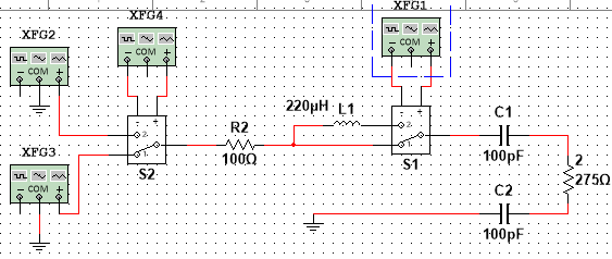
I am working on a circuit that transmits ~1MHz sine wave(20V amplitude) in RLC based circuit scheme, also transmits high-frequency signals(pulses(non-periodic)) ~20MHz(10 %DS)(20V) in a CR-based circuit scheme. The circuit involves 'disabling' of inductor for ~20MHz signal transmission for a short amount of time(say 10% of the enabled time).
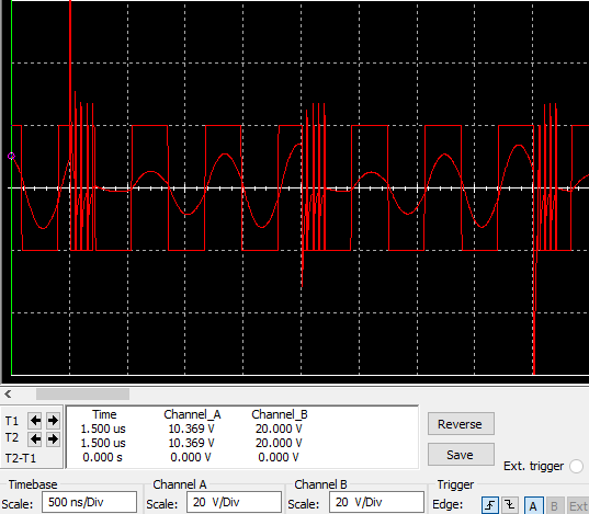
I'm having problems in suppressing the voltage spikes(~ +-100 V) which are generated the moment I disable the inductor AND after I connect the wire, while the rest of the time the circuit behaves alright. NOTE: I'm measuring the differential voltage across Resistor(275ohm)

XFG3: 20MHZ, 10%DS +- 20V square wave
XFG2: 1.58MHz(RLC resonant), 50%DS, +- 20V square wave
XFG4,1: 500KHz, 10%DS
Desired output: Maximum power transfer at 275ohms(after rectification, filter) + High-speed data transmission(to be demodulated later from 275ohms)
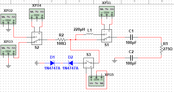
So, to tackle that, I came up with an idea to temporarily enable the pair of opposite Zener diodes which would act as a voltage limiter(say +-20V) right after the switch S1, but it found to be unsuccessful. I can still see the surges. Also, I've read that Zener has high capacitance, so it won't be effective in a high speed temporarily switching(Note that I want to enable the voltage suppression device momentarily for the initial surge protection(~10ns))


I also have an idea to make my switch kind of a hybrid-relay based, where there will be a state for a very short period of time (just after inductor open-circuit and before connecting the wire) to absorb the surges. But, I'm not getting effective ideas.
I also have heard about MOVs. But I'm not sure about its effectiveness as they also possess capacitance. It's not available in NI Multisim, so I am not sure if it's good.
I need some suggestions/ways to tackle the problem. NOTE: C1 capacitor is an instrument that is very delicate and it's a must to suppress any kind of spike just before it

