1
\$\begingroup\$

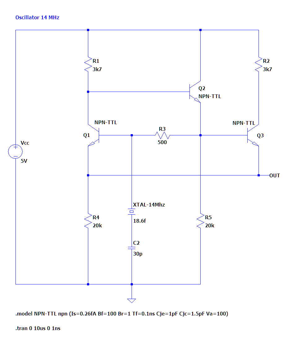
I came across this oscillator circuit.

enter image description here

I can't figure out how it works. Ok, there is a differential pair Q1, Q3 with a tail resistor R4... Everything else is out of my comprehension (it doesn't resemble any oscillator topology I'm familiar with). Any help would be appreciated.

Edit 1:

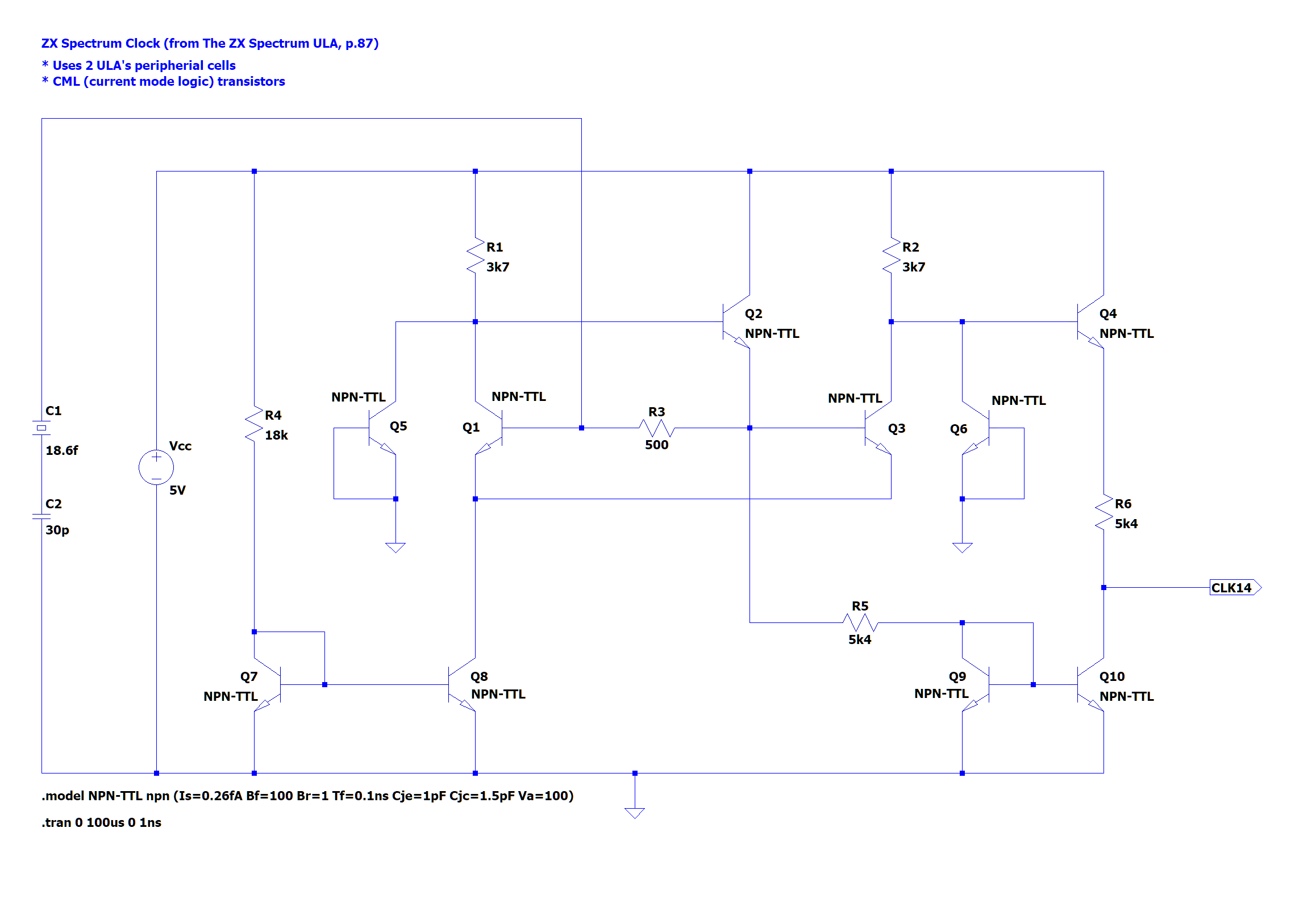
Source: The schematic above is a simplified version of the ZX Spectrum's (legendary British microcomputer) clock circuit. Here is the 'full' version:

enter image description here

For the simplified version, the current mirrors have been replaced with resistors and the second stage has been removed.

The circuit was published in the excellent book 'The ZX Spectrum ULA' by Chris Smith. He reverse-engineered the chip using a microscope! Although the book describes clock interworkings, I found it difficult to understand.

Components: for the actual circuit, there are only two external components: 14 MHz crystal and 30pF capacitor. All other elements are part of the ULA chip (Ferranti 6C000 - kind of an old-time ASIC). The 'full' circuit deploys two (of 48) 'peripheral' cells (the chip has also a bunch of 'matrix' cells).

I haven't been able to find any relevant characteristics of those BJTs - the ULA uses a less-known current-mode-logic (CML). After some trial and error, the LTSpice model started to oscillate with a TTL-type transistor.

\$\endgroup\$
6
  • 1
    \$\begingroup\$ If Q1 and Q3 are to be considered as a differential pair, the tail resistor is R4, not R5. \$\endgroup\$
    – Hearth
    Commented Jun 8, 2023 at 14:42
  • \$\begingroup\$ Question: Is there any reference (book, article,...) regarding this oscillator type? \$\endgroup\$
    – LvW
    Commented Jun 8, 2023 at 18:27
  • \$\begingroup\$ @Hearth: thx, I've fixed the mistake in the original text. \$\endgroup\$
    – RayX
    Commented Jun 9, 2023 at 16:47
  • \$\begingroup\$ @LvW: see 'Edit 1' above. \$\endgroup\$
    – RayX
    Commented Jun 9, 2023 at 16:47
  • \$\begingroup\$ When you say "current-mode logic" do you mean ECL perhaps? That's very common for very high-speed logic, especially in the time period the ZX Spectrum is from. \$\endgroup\$
    – Hearth
    Commented Jun 9, 2023 at 16:50

2 Answers 2

2
\$\begingroup\$

I know many different oscillator circuits - however, I must confess that the shown version is new for me. Nevertheless, with the oscillation condition in my mind, it should not be a problem to describe the basic working principle.

  • Without the crystal and the 30p capacitor we have (1) a negative DC feedback loop across Q1(collector)-Q2-R3-Q1(base). This is good for stabilization of the DC operating points. At the same time, there is (2) another DC feedback loop active formed by Q1(collector)-Q2-Q3-Q1 (emitter). However, this is a positive DC fedback loop - however, with a rather small feedback signal (if compared with case (1)). This is due to the comparable low input resistance at the emitter node (if compared with the base input resistance). That means: DC negative feedback dominates (loop (1)).

  • Now the crystal path comes into playe. There is one single frequency wo (series resonance) which grounds the base of Q1. As a consequence, for this frequency wo the transistor Q1 works in common base configuration and the feedback loop (1) is not active for wo (base node grounded for wo). However, the remaining positive feedback loop across Q3 is the only one which is active and can fulfill the oscillation condition (provided the loop gain >= unity for one frequerncy.)

\$\endgroup\$
1
  • 2
    \$\begingroup\$ Perhaps this oscillator might be an integrated-circuit type where pin count is important. The only external pin needed connects to the crystal, unlike other Pierce crystal oscillators that need two external pins. Also supported by TTL nomenclature, and the NPN-only transistors. Neat! \$\endgroup\$
    – glen_geek
    Commented Jun 8, 2023 at 16:29
1
\$\begingroup\$

The XTAL is "charged" via 500R when the XTAL is in positive cycle , and "cutted" from this charge during negative cycle.
During positive cycle when XTAL is charged the Q3_base is little higher then Q1_base because of voltage across 500R. That causes a tittle closing of Q1 and thus opening the charging transistor Q2.
During negative cycle the voltage levels of the bases are switched (Q1 higher, Q3 lower) so charging transistor Q2 is closed.

\$\endgroup\$

Your Answer

By clicking “Post Your Answer”, you agree to our terms of service and acknowledge you have read our privacy policy.

Not the answer you're looking for? Browse other questions tagged or ask your own question.