0
\$\begingroup\$

I am trying to design an ultra-low-noise pre-amplification stage for a MEMS. The amplification consists of a non-inverting amplifier specifically chosen to have less than 4 nV/sqrt(Hz) as input voltage noise. The MEMS is on a separate PCB connected to the amplifier PCB via an SMA connector.

I read multiple times that such low noise circuits should be placed in a metallic enclosure to avoid picking up electromagnetic interference. In some cases, the case is not grounded. Does the shielding still work then? If it's grounded, doesn't that introduce a parasitic capacitor between the traces and the grounded shield, for example?

Edit 1:

The MEMS has a piezoelectric transducer that is modeled by the photodiode equivalent circuit. The sensor output current is in the order of ~200nA with a frequency up to 1MHz which creates a couple of constraints in my circuit:

  1. The input capacitance should stay as low as possible to avoid the partitioning of the current and thus a decrease in the voltage at the non inverting input of the op-amp.

  2. The noise should be kept as low as 4nV/sqrt(Hz). Thus the low feedback resistors.

  3. Have as low input bias current as possible to avoid saturating the op-Amp
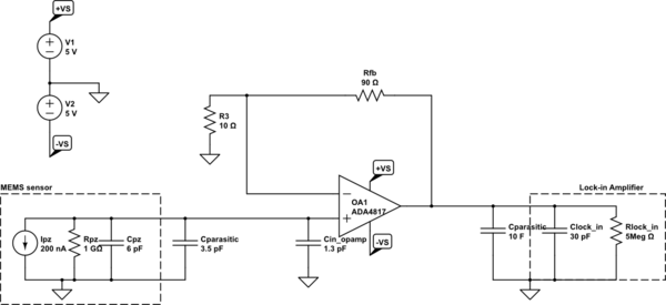
schematic

simulate this circuit – Schematic created using CircuitLab

Note: The 3.5pF capacitor at the input is due to the SMA connector (the 2 PCBs will be connected directly to each other via a female-male SMA connection.) The 10pF capacitor at the output is due to the coaxial cable.

\$\endgroup\$
1
  • \$\begingroup\$ It can be a good idea, yes. I'm afraid there isn't enough information here to determine whether is is in your particular case. Please describe the nature of your source (signal level, bandwidth, impedance, cabling type and length, grounding at either end if applicable), and load (same considerations). \$\endgroup\$ Commented May 5 at 19:50

4 Answers 4

0
\$\begingroup\$

low noise circuits should be placed in a metallic enclosure to avoid picking up electromagnetic interference. In some cases, the case is not grounded. Does the shielding still work then? If it's grounded, doesn't that introduce a parasitic capacitor between the traces and the grounded shield, for example?

Short answer: Yes, grounded shielding will introduce parasitic capacitance between the traces and ground, which may cause problems such reduced high-frequecy response or unstable behaviour.

One solution to this problem is to run an active guard ring as a shield around the sensitive traces. This "active guard ring" should not be grounded, it should be connected to a node that is a low-impedance buffered version of the sensitive signal trace voltage (hence the term "active"). This minimises the voltage difference between the sensitive trace and the guard ring, thus minimising any parasitic current flow between them (due to either parasitic capacitance, or surface currents on the PCB materials). The idea being that parasitic capacitive current due to a grounded shield will then flow from the active guard ring, not the sensitive trace.

Here are some links that may be helpful:

https://electronics.stackexchange.com/a/24890/341959

What are Guard Rings?

https://electronics.stackexchange.com/a/594576/341959

https://www.analog.com/media/en/technical-documentation/application-notes/41727248an_347.pdf

\$\endgroup\$
3
  • 1
    \$\begingroup\$ The cable equivalent of this is a triaxial cable--they're quite expensive, but essential for certain types of measurement. \$\endgroup\$
    – Hearth
    Commented May 6 at 0:38
  • \$\begingroup\$ @Hearth Agreed. The other option the OP should consider having the amplifier installed with the sensor to avoid such issues altogether. But that requires more lines on the cable: power, and signal. No free lunch, I guess. \$\endgroup\$ Commented May 6 at 0:40
  • \$\begingroup\$ Thank you very much for your suggestion. \$\endgroup\$
    – jrad
    Commented May 6 at 11:55
0
\$\begingroup\$

In many cases it's hard to tell ahead of time whether you're going to have a problem with noise or other coupling (like unintended feedback) into a sensitive circuit.

What we sometimes do, based on past experience, is to make provisions for a metal hut to enclose the sensitive circuit. This usually takes the form of a ground ring around the circuit, that the metal cover can be soldered to.

One unintended consequence of this is that, depending on the frequencies involved, you may create a cavity that resonates at certain frequencies. We had this issue with some 16 GHz amplifier stages that were designed, and had to "de-tune" the cavity by making it non-rectangular.

\$\endgroup\$
1
  • \$\begingroup\$ Thank you for your intake. I am not sure I understand the last part of your answer involving resonating cavities. Can you please develop on how that works \$\endgroup\$
    – jrad
    Commented May 6 at 11:58
0
\$\begingroup\$

If there is any DC component to the signal current source the input voltage to the op amp will rise (or fall) and the op amp will saturate.

Very low feedback resistors is an extreme choice, even if the op amp can supply enough current. I would use more moderate values just on general principles. Unless an actual calculation of the thermal noise shows that it is necessary.

Grounding and noise/ interference is a very complex topic. I suggest taking the expedient approach of putting the op amp in a metal box with the SMA connector shield connected to the metal box.

Think about the power supplies which might contribute noise. For the ultimate in low noise use batteries inside the metal box.

I have found the book by Ott to be useful in thinking about noise and interference, although I admit I have only worked through selected sections. Oddly enough, available as a free download, google ott noise and grounding

\$\endgroup\$
1
  • \$\begingroup\$ Thank you for your response. Do you know how I can block the DC component from the non inverting input of the op Amp? \$\endgroup\$
    – jrad
    Commented May 5 at 21:47
0
\$\begingroup\$

You will find cables your worst enemy. The transducer has to be in a shielded enclosure together with a buffer stage before anything goes onto a cable. The buffer stage’s non-inverting input has to be connected to the sensor with the shortest possible conductor. Ideally you would lift the pin of the op-amp and connect it to the adjacent sensor using a wire up in the air. Imagine the wire being way 10mm long at most.

That way, you’ll be at a design point where literally nothing can be done any better other than getting the op-amp in die form and wire bonding it to the sensor without having to deal with package conductance (and there always is some!).

Once this limiting case works, you can proceed at making things worse and seeing if it still works well enough.

\$\endgroup\$
1
  • \$\begingroup\$ Thank you for your answer. Unfortunately the sensor PCB is already fabricated and I am afraid I cannot change that. But if you have any idea on how to cancel out the cable capacitance that will be of great help :) \$\endgroup\$
    – jrad
    Commented May 6 at 12:01

Your Answer

By clicking “Post Your Answer”, you agree to our terms of service and acknowledge you have read our privacy policy.

Not the answer you're looking for? Browse other questions tagged or ask your own question.