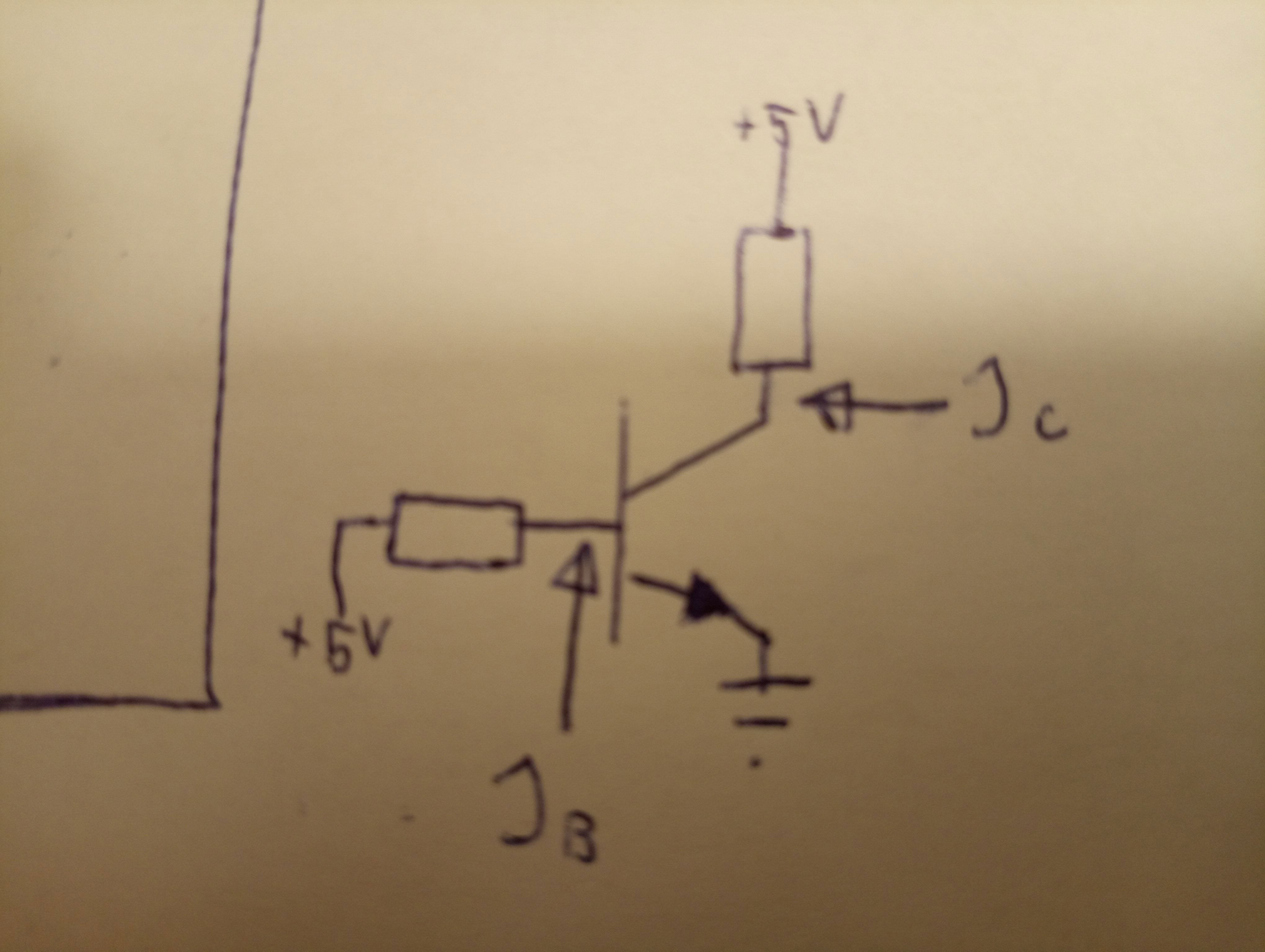
I am very new to transistors unfortunately, so sorry if I don't know every formula already. The thing is, I would like to use a bipolar NPN transistor as an amplifier. It has a current gain of 200. The Collector does drain the current it is supposed to and the emitter outputs the correct current, but I have a question with the Base current. Suppose we have a 5 V supply both at the C and B. There is also a resistor at the B and another at C. Using a simulator, it draws way less current than the calculation I did with Ohm's law. I also found out that the resistor at C plays a role here. My question is how does the resistor at C affect the current at B?
-
\$\begingroup\$ Current Ib = 8.57 mA = (5-0.7)/470. What is the problem? It is a way too "high". Ic should be more than 300 mA. What is the power supply? No resistor side collector is not advised. \$\endgroup\$– Antonio51Commented Sep 1 at 17:14
-
\$\begingroup\$ Sorry, I misaked the question. \$\endgroup\$– Vargánya MűvekCommented Sep 1 at 17:24
4 Answers
Why does collector resistance \$R_C\$ affect base current? The answer is it doesn't, at least not much. You've just got something wrong somewhere. There's always a slight dependence of anything on everything else, so nothing in the universe is truly independent, and you can expect some fluctuation, but base current is largely independent of collector current.
It sounds like you are lost. The answer lies in the maths, and you have to do the maths to understand. It's OK to guess resistor values, and learn from your mistakes, but it's better to start on a solid foundation of understanding. So, what follows is adapted from a primer & execise sheet I wrote for my students on day one of transistor stuff.
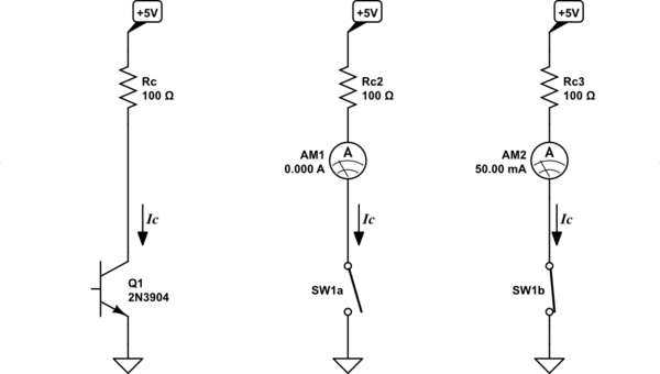
The transistor can be switched fully off (cut-off), fully on (saturated) or somewhere in between. Considering only the fully-on or fully-off states, for the moment, we can get some valuable information to use later. Pretend that the transistor is a switch, and ignore anything happening at the base for now:
simulate this circuit – Schematic created using CircuitLab
Middle and right I emulate the the transistor conditions cut-off (middle, where it behaves like an open switch) and saturated (right, where it behaves like a closed switch). Collector current is measured by ammeters. Obviously with the switch open (cut-off) no current can pass:
$$ I_{C(CUT)} = 0 $$
However, the right-hand "saturated" model demonstrates that current can never exceed some maximum, predicted by Ohm's law:
$$ I_{C(SAT)} = \frac{5V}{R_C} = 50mA $$
If you wanted some other saturation current, you use that same equation to find an appropriate resistance. Next we consider base current, and how we'll calculate and control it:
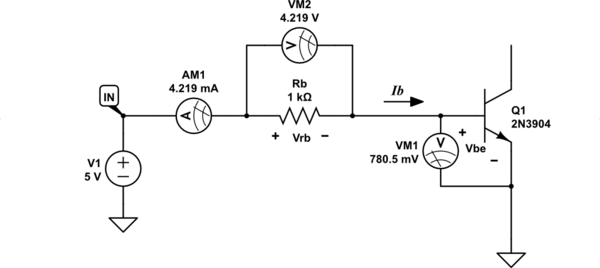
When this transistor is saturated or operating in its linear region, the potential difference between its base and emitter will be about 0.7V. It's actually a little more here, and it can vary between 0.5V and 0.9V depending on various things like transistor model and base current, but people generally say \$V_{BE}\approx 0.7V\$. We'll do the same here.
Kirchhoff's Voltage Law tells us that the sum of \$V_{BE}\$ and the voltage \$V_{RB}\$ across the base resistor must be the same as the difference between the potentials at each end:
$$ \begin{aligned} V_{RB} + V_{BE} &= V_{IN} - 0V \\ \\ V_{RB} + 0.7V &= +5V - 0V \\ \\ V_{RB} &= +5V - 0.7V \\ \\ &= 4.3V \end{aligned} $$
Using Ohm's law again, we can predict the current through \$R_B\$, which ends up entering the base, and which we call "base current" \$I_B\$:
$$ \begin{aligned} I_B &= \frac{V_{RB}}{R_B} \\ \\ &= \frac{4.3V}{1k\Omega} \\ \\ &= 4.3mA \end{aligned} $$
The simulation shows 4.3mA, the difference being due to the estimation \$V_{BE}=0.7V\$. Otherwise everything checks out.
Now let's put everything together and relate these two currents \$I_C\$ and \$I_B\$:
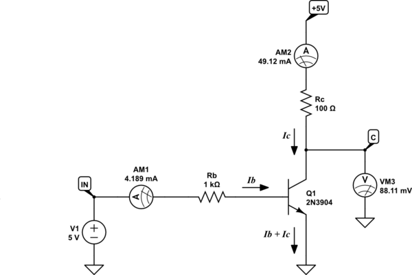
In the books it says:
$$ I_C = \beta \times I_B $$
My simulated transistor has a current gain \$\beta\$ (sometimes called \$h_{FE}\$) \$\beta = 140\$. From that you might therefore assume that:
$$ \begin{aligned} I_C &= 140 I_B \\ \\ &= 140 \times 4.3mA \\ \\ &= 0.6A \end{aligned} $$
That's impossible, as we already established that collector current can't exceed \$I_{C(SAT)}=50mA\$. Therefore, this transistor is completely and utterly saturated, and passing the maximum collector current possible. If you look closely at the simulated circuit above, you can see that collector-to-emitter voltage \$V_{CE}\$ is slightly above 0V, which tells you that a bipolar junction transistor is not a perfect switch. A perfect 0Ω switch would have zero volts across it. We generally assume that a saturated transistor will have \$V_{CE}=0.1V\$, or for some devices \$V_{CE}=0.2V\$. Because of this, our estimated \$I_{C(SAT)}\$ was a little optimistic, but that's of little consequence here, we were close enough.
Let's try to take the transistor out of saturation. There are several ways to do this:
Reduce \$R_C\$. This will increase \$I_{C(SAT)}\$, and if we increase \$I_{C(SAT)}\$ to well over 0.6A, that would work.
Reduce \$V_{IN}\$. This would reduce base current \$I_B\$.
Increase \$R_B\$. This would also reduce \$I_B\$.
Since you are using a fixed \$V_{IN}=+5V\$, I'll try to find a value for \$R_B\$ that will place the transistor half-way between cut-off and saturation, which occurs at:
$$ I_C = \frac{I_{C(SAT)}}{2} = 25mA $$
First find the corresponding base current necessary in this state:
$$ \begin{aligned} I_C &= \beta I_B \\ \\ I_B &= \frac{I_C}{\beta} \\ \\ &= \frac{25mA}{140} \\ \\ &= 180\mu A \end{aligned} $$
There's no point using figures with more than two significant digits, since everything is somewhat approximate. We use the KVL equation from before, together with Ohm's law, to obtain a suitable resistance \$R_B\$:
$$ \begin{aligned} I_B &= \frac{V_{IN}-V_{BE}}{R_B} \\ \\ R_B &= \frac{5V - 0.7V}{I_B} \\ \\ &= \frac{4.3V}{180\mu A} \\ \\ &= 24k\Omega \\ \\ \end{aligned} $$
Replace the 1kΩ resistor with 24kΩ:
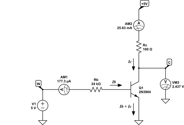
That's perfect. We have 25mA of collector current, and \$V_{CE}\$ is now half of the supply.
The next question is how to know the \$\beta\$ of your own transistor in real life, it's crucial for all those calculations. Glad you asked. You don't know, until you measure it, so measure it. Start with setting base current to something small, like 100μA:
$$ \begin{aligned} R_B &= \frac{5V - 0.7V}{I_B} \\ \\ &= \frac{4.3V}{100\mu A} \\ \\ &= 43k\Omega \\ \\ \end{aligned} $$
That's a hard resistance to find, so let's use 47kΩ instead:
$$ \begin{aligned} I_B &= \frac{4.3V}{47k\Omega} \\ \\ &= 91\mu A \\ \\ \end{aligned} $$
Now choose a collector resistor \$R_C\$. You could guess and try different values, but the intelligent approach is to assume high current gain \$\beta=300\$, and calculate the resistance that would develop 2V or so with the corresponding collector current passing through it:
$$ \begin{aligned} I_C &= \beta I_B \\ \\ &= 300 \times 91\mu A \\ \\ &= 27mA \\ \\ R_C &= \frac{2V}{27mA} \\ \\ &= 74\Omega \\ \\ \end{aligned} $$
74Ω is another tough value to find, so I'll use 68Ω instead. It's not important to be exact here. Build the circuit, and measure the voltage across \$R_C\$:
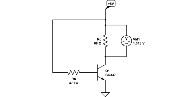
To find \$\beta\$ we need to know both base current \$I_B\$ and collector current \$I_C\$. Base current has been set already, \$I_B=91\mu A\$, but collector current can be calculated from our measured voltage across \$R_C\$, using Ohm's law:
$$ \begin{aligned} I_C &= \frac{V_{RC}}{R_C} \\ \\ &= \frac{1.32V}{68\Omega} \\ \\ &= 19mA \\ \\ \end{aligned} $$
Now we find the ratio \$\beta\$ of the two currents:
$$ \begin{aligned} I_C &= \beta I_B \\ \\ \beta &= \frac{I_C}{I_B} \\ \\ &= \frac{19mA}{91\mu A} \\ \\ &= 209 \end{aligned} $$
Choosing a base current depends what the load is and what frequency the load is driven, another words how much time is allowable the Bjt stays in linear region during switching. A higher base current -> faster switch (until some point like Ib>Ic/10).
The Vbe of the transistor will be about 0.7V so you can expect the base current to be roughly (5V-0.7V)/470Ω = 9.1mA. Since the base current is relatively high Vbe might be higher, and therefore the current might be a bit less, depending on the transistor. If it's a small type like 2N3904 it will definitely be much less Ib than 9.1mA since Vbe will be closer to 900mV.
Let's do a CircuitLab simulation with a power transistor TIP41:
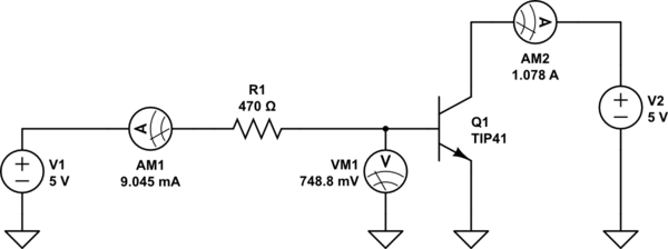
simulate this circuit – Schematic created using CircuitLab
Now the transistor had better have a pretty good heat sink or it will die in this configuration since it's dissipating >5W.
Also Vbe will drop as the transistor heats, this is indicative of what would typically happen with a real TIP41 in this circuit for the first brief period after power is applied.
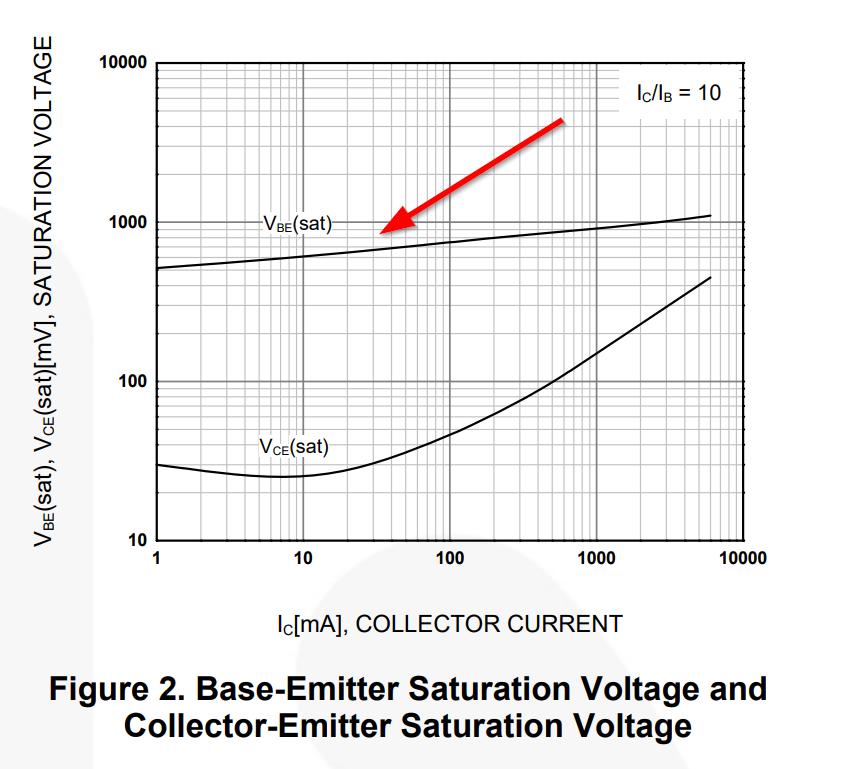
To predict the Vbe from the datasheet, there are curves, but for normal saturated switching operation, which don't exactly apply in your situation with the transistor out of saturation:
As you can see the predicted Vbe in saturated condition and 9mA Ib is around 50mV less than the simulated solution out of saturation. Still pretty close though.
Ignoring odd arrangements, there are two cases that have very different results with BJTs: (1) operated as an amplifier (active mode); and, (2) operated as a switch (saturated mode).
Technically, these can be analyzed using a single, rather complex model. (See the DC version of the Ebers-Moll model.) But for ease of analysis, these are instead usually broken into two different modes with two different behaviors.
If you already know the circuit's purpose, then you can just take the assumptions for that purpose and start there. If the numbers work out then you are done. If you don't know the circuit's purpose (or it is a test to see if you can work things out, either way), then you usually start with the active mode assumptions and see if the results are consistent. If so, done. If not, you switch over to the saturated mode assumptions and re-compute. (Of course, you could do it in the other order.)
One or the other will result in a consistent result and you will know the mode of operation and quantities that will be close to what will be measured.
(The following does not apply to Darlington arrangements.)
When writing below, I'll be providing magnitudes (unless you see a specific minus sign.) You need to apply them appropriately, depending upon NPN or PNP situations....
active mode assumptions
The collector acts like a current sink (NPN) or source (PNP) with infinite impedance.
(This is wrong due to the Early Effect. But since the Early Effect generates only about a 1% error, it can usually be ignored.)
The bipolar will have a relatively unchanging ratio during operation, \$\beta=\frac{I_{_\text{C}}}{I_{_\text{B}}}\$.
(While any two different bipolars from the same family of devices will have different values, they will be within 30-50% of each other. For small signal devices without a datasheet you can expect \$100 \le \beta\le 350\$. But check the datasheet for details, if available. For large signal devices without a datasheet you can expect \$10 \le \beta\le 60\$. But check the datasheet for details, if available. \$\beta\$ will depend upon the device temperature and quiescent operating current. But given some specific temperature and quiescent operating current, you can expect this value to remain relatively flat (fixed.))
The bipolar will have a relatively unchanging \$V_{_\text{BE}}\$ at any given quiescent operating current.
(While any two different bipolars from the same family of devices will have different values, yet again, they will be within about \$50\:\text{mV}\$ of each other when operating at the same quiescent point. Without a datasheet and without knowing the operating point you can expect \$450 \le V_{_\text{BE}}\le 950\$ at room temperature. But check the datasheet for details, if available. \$V_{_\text{BE}}\$ will depend upon the device temperature and quiescent operating current. But given some specific temperature and quiescent operating current, you can expect this value to remain relatively flat (fixed.) Over wide temperature changes, you can expect to see something in the area of about \$-2\frac{\text{mV}}{^\circ\text{C}}\$ change. Over wide operating current changes and with small signal devices, you can expect to see about \$60\:\text{mV}\$ change per decade change in collector current. For large signal devices this may be more like \$100\:\text{mV}\$ change per decade change, but they usually start at a lower \$V_{_\text{BE}}\$, too. Again, look at the datasheet to get a better idea.)
One enters into analysis of an existing circuit with some idea of \$V_{_\text{BE}}\$ (for some estimated collector current and operating temperature) and \$\beta\$, and makes adjustments later as calculations reveal their results.
saturated mode assumptions
The collector acts like a voltage source with zero impedance.
(This, again, isn't strictly true. Usually, there are some small bulk impedances at the collector, emitter, and base.)
\$V_{_\text{BE}}\$ will be marginally higher than in active mode -- perhaps \$50\:\text{mV}\$ higher, maybe a little more.
\$V_{_\text{CE}}\$ is relatively constant and small. Typically the saturated \$V_{_\text{CE}}\le 200\:\text{mV}\$.
example circuit
None of the values are specified below. Just the topology, for now:
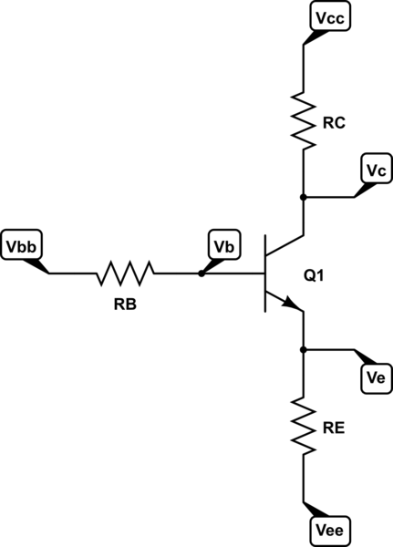
simulate this circuit – Schematic created using CircuitLab
Three resistor values need to be specified, along with three ideal voltage source values. Once those are known, the situation can be worked out.
In the following, I'll start by assuming active mode and room temperature.
- \$V_{_\text{CC}}=10\:\text{V}\$
- \$V_{_\text{EE}}=-10\:\text{V}\$
- \$V_{_\text{BB}}=-8\:\text{V}\$
- \$R_{_\text{B}}=10\:\text{k}\Omega\$
- \$R_{_\text{C}}=1\:\text{k}\Omega\$
- \$R_{_\text{E}}=100\:\Omega\$
- \$\beta\approx 150\$
- \$V_{_\text{BE}}\approx 700\:\text{mV}\$ at \$I_{_\text{C}}=2\:\text{mA}\$
KVL provides \$I_{_\text{B}}=\frac{V_{_\text{BB}}-V_{_\text{BE}}-V_{_\text{EE}}}{R_{_\text{B}}+R_{_\text{E}}\cdot\left(\beta+1\right)}\approx 51.8\:\mu\text{A}\$. So \$I_{_\text{C}}=\beta\cdot I_{_\text{B}}\approx 7.77\:\text{mA}\$ and \$I_{_\text{E}}\approx 7.82\:\text{mA}\$. Also, \$V_{_\text{B}}\approx -8.52\:\text{V}\$, \$V_{_\text{E}}\approx -9.22\:\text{V}\$, and \$V_{_\text{C}}\approx 2.23\:\text{V}\$.
Suppose, instead, we happened to pick out a bipolar with \$\beta=200\$, instead. Then, \$I_{_\text{B}}\approx 43.2\:\mu\text{A}\$, \$I_{_\text{C}}\approx 8.64\:\text{mA}\$ and \$I_{_\text{E}}\approx 8.68\:\text{mA}\$, \$V_{_\text{B}}\approx -8.43\:\text{V}\$, \$V_{_\text{E}}\approx -9.13\:\text{V}\$, and \$V_{_\text{C}}\approx 1.36\:\text{V}\$.
As you can see, some but not much change. And regardless, the bipolar actually has the collector voltage above the base voltage. So it is in active mode, as assumed.
Note: The current is almost 5 times higher than what I assumed for the base-emitter voltage. This would mean that \$V_{_\text{BE}}\approx 741\:\text{mV}\$, instead. A few more details would change. (You can work it out.) But this circuit would still be in active mode and the analysis would be close to what you'd experience if you built this on a solderless breadboard.
Now suppose everything else stays the same except that \$V_{_\text{BB}}=-5\:\text{V}\$, instead? A quick check says that \$I_{_\text{B}}\approx 171\:\mu\text{A}\$ and \$I_{_\text{C}}\approx 25.7\:\text{mA}\$. This would set \$V_{_\text{B}}\approx -6.71\:\text{V}\$ and \$V_{_\text{C}}\approx -15.7\:\text{V}\$! This last value, \$V_{_\text{C}}\approx -15.7\:\text{V}\$, immediately tells you that it just cannot be right and therefore this must be a saturated situation, instead.
This means you now ignore \$\beta\$. It's very wrong and cannot be used. Instead, you now apply the saturated \$V_{_\text{CE}}\le 200\:\text{mV}\$ and \$V_{_\text{BE}}\approx 750\:\text{mV}\$, to start out. A very quick assumption would be to compute \$\frac{10\:\text{V}-\left(-10\:\text{V}\right)-200\:\text{mV}}{1\:\text{k}\Omega+100\:\Omega}=18\:\text{mA} \$ for the collector and emitter currents. That misses including the base current into the emitter current -- you know the emitter current will be a little more than the collector current. If you more carefully solve this out you will get \$I_{_\text{C}}\approx 18\:\text{mA}\$ and \$I_{_\text{E}}\approx 18.2\:\text{mA}\$. The collector and emitter voltages will be very close to each other, as expected.
My question is how does the resistor at C affect the current at B.
If the collector resistor gets large enough, it will force the collector voltage down very close to the emitter voltage, forcing the bipolar into saturation. Make it a lot smaller and the bipolar will move back into active mode.
-
\$\begingroup\$ Thank you, but why do I need to apply negative voltage at Vbb? \$\endgroup\$ Commented Sep 2 at 16:02
-
\$\begingroup\$ @VargányaMűvek You don't. It can be zero. I just picked that to make another point. \$\endgroup\$ Commented Sep 2 at 19:57
-
\$\begingroup\$ Note that Beta = delta(Ic) / delta(Ib) and not Ic/Ib ... \$\endgroup\$ Commented Sep 4 at 14:04

