1
\$\begingroup\$

I designed my first PCB in Fritzing, intending to have it milled at the local hackerspace (they want Gerber files) and then assemble it with THT components.

But now all the copper is on the top side (milling two-sided PCBs is apparently way more complicated and unnecessary for such a simple circuit), and the holes are set up so that the components have to go on top, too!
The resistors and linear regulators aren't a problem, they are symmetrical, but the RJ45 connector and the Max485 chip are not!

Is there a way to mirror the copper traces (never mind the silk screen, it's not gonna get milled anyway!)?
Fritzing doesn't seem to have the option, but it can export Gerber files.

Thanks!

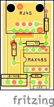
This is the PCB, btw:

PCB as it is right now, not suitable for THT assembly

\$\endgroup\$
5
  • 4
    \$\begingroup\$ "Fritzing doesn't seem to have the option" - sounds like a good reason to ditch it and use a real EDA. There are free options, for example kicad.org [Edited by a moderator.] \$\endgroup\$ Commented Apr 22, 2016 at 9:27
  • \$\begingroup\$ The converter for the CNC mill should be able to mirror gerber files in order to process backsides. \$\endgroup\$ Commented Apr 22, 2016 at 9:28
  • 4
    \$\begingroup\$ See, there is a reason why fritzing has a bad reputation among electronics and electrical engineering professionals, students, and enthusiasts. \$\endgroup\$
    – PlasmaHH
    Commented Apr 22, 2016 at 9:31
  • 1
    \$\begingroup\$ Don't use Fritzing. It's pure garbage. \$\endgroup\$
    – DerStrom8
    Commented Apr 22, 2016 at 12:40
  • 1
    \$\begingroup\$ @PlasmaHH & DmitryGrigoryev: If you want to rant about Fritzing you should select an appropriate example :). Gerber data is always viewed from top of the stack. Regardless which EDA-SW produced it. (PADS, Eagle...) There is no need to mirror a layer at any time. So lacking this feature doesn't make Fritzing a bad SW. After all it's an electronics learner's tool, not an EDA software :) \$\endgroup\$
    – Ariser
    Commented Apr 24, 2016 at 8:51

2 Answers 2

1
\$\begingroup\$

If I understand your problem correctly, you do not need to mirror your copper layer.

Consider a "real" layout with a "real EDA" software like Eagle or PADS. The layers have to have the same coordinate system and

The output with coordinates are always orientated as if you are looking onto the populated side of your PCB. Otherwise it would be rather difficult to align the layers correctly.

So the bottom layer has to be mirrored by the manufacturer anyway. Because of this I assume your guys at the hackerspace just can take the top layer, declare it as a bottom layer and it will be mirrored by the CAM software correctly.

For viewing the Gerber files to identify all layers correctly I recommend the free tool GCPreview.

\$\endgroup\$
1
\$\begingroup\$

you will find a option under the PCB tab as EXPORT FOR PCB along side auto route and other options.. click on it.. and select (etchable pdf). then provide a save location say desktop and a 10 to 15 pdf will be saved on the location. find the pdf which contains the copper tracks bottom layer (mirror) and take the print out.

\$\endgroup\$
1
  • \$\begingroup\$ This doesn't help if the board will be milled, as they will need the actual Gerber files to feed into the control software. \$\endgroup\$ Commented Sep 23, 2016 at 23:12

Your Answer

By clicking “Post Your Answer”, you agree to our terms of service and acknowledge you have read our privacy policy.

Not the answer you're looking for? Browse other questions tagged or ask your own question.