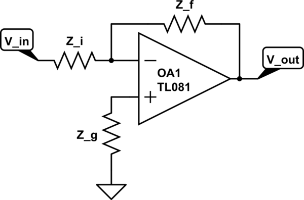
Why people use \$Z_g\$ in the following circuit:

simulate this circuit – Schematic created using CircuitLab
As \$Z_g\$ doesn't appear in \$V_{out}\$ equation: \$-Z_f/Z_i \times V_{in}\$
Why people use \$Z_g\$ in the following circuit:

simulate this circuit – Schematic created using CircuitLab
As \$Z_g\$ doesn't appear in \$V_{out}\$ equation: \$-Z_f/Z_i \times V_{in}\$
The resistor Z_g is sometimes needed to keep the DC offset of the amplifier as low as possible.
Imagine that Z_g was not present, then the + input of the opamp is always 0 V. Most opamps have a small DC input current flowing into or out of the inputs, see the datasheet how much this is. This small current will flow through Z_i and / or Z_f and it will cause a voltage drop across these resistors. This causes an offset error at the - input. To introduce a similar error at the + input, Z_g is used, it usually has a value which is the value of Z_i and Z_f in parallel. Now both inputs have the same offset error due to the input biasing current, the opamp only amplifies the voltage difference, we just eliminated that difference, now the offset (due to the input biasing currents) is gone !
For an explanation by Dave Jones, see the EEVBlog about opamps
As the others mentioned, for the TL081 this is not such an issue as it has JFET inputs. Also opamps with MOS inputs do not suffer from this. Mostly for opamps with BJT inputs this Z_g is needed, opamps like the 741 or NE5532 for example.
The resistor Z_g is there to ensure that the offset voltage at the positive and negative terminals of the opamp is as close to identical as possible (hence not affecting the circuit, as it appears as common-mode offset).
By making the input bias current at each terminal (which should be approximately the same) flow through identical impedances, you should end up with the same voltage offset at each node. Hence Z_g is calculated to equal the same impedance as would be seen "looking out of" the inverting input:
\$Z\_g = Z\_i || Z\_f = {{Z\_i\times Z\_f} \over {Z\_i + Z_f}} \$
As Brian Drummond points out, with the TL081 having a JFET input stage and an input bias current that you would need very expensive equipment to measure, practically speaking it is likely to be redundant in this particular schematic.
However, it is also likely that since the TL081 is the default opamp selected by CircuitLab when drawing a schematic I imagine that your original schematic may be for a different device, where this technique has a greater effect.
Z_i and Z_f in parallel in Z_g calculation?
\$\endgroup\$